How to run simulations
Workflow
The essential workflow to run simulations with Quokka3 consist of 3 separate steps:
- Define your simulation input parameters in a settingsfile within a text-editor of your choice (Notepad++ is a good choice).
- Start the simulation and manage cloud simulations via the Quokka3-client software, using either the GUI or the command-line. For larger cloud simulations, the recommended way is to start the simulation, disconnect, and retrieve the results once finished.
- Post-process the results via the GUI’s basic plotting functionality, or by processing the output files yourself.
The core of Quokka3 which performs the actual simulations, called Quokka3-core, comes in two ways:
- a restricted free version, which is included as a standalone executable in Quokka3-client
- the paid versions, which exclusively run as a cloud-service controlled via Quokka3-client, and consequently require internet connection.
The way of controlling simulations in Quokka3-client is (almost) identical regardless whether you use the included free version or the cloud-service. Only for using the cloud-service, one needs to have signed up for a user account.
Note that for the cloud, it sometimes might take up to a couple of minutes for the simulation to start. This has to do with automatic scaling of cloud-servers and is currently not entirely avoidable. The scaling algorithms are however monitored and optimized in such a way that only very rarely this delay should be significant compared to the overall simulation time. It should be a few minutes at maximum.
If a connected cloud-simulation finishes or a finished cloud-simulation is opened, the results are automatically downloaded and deleted from the cloud. Only some anonymous data like simulation time, memory usage etc., are kept for statistical and service-improvement purposes.
System requirements
Installation of Quokka3-client is required both for free and paid-version usage, which notably does not require admin rights. It is currently available for Windows 64bit only. As the included standalone free Quokka3-core version allows only small simulations, and large simulations are exclusively performed in the cloud, Quokka3 doesn’t require highly performant computer hardware for simulations. It should work on any reasonable up-to-date PC with Windows 7,8 or 10.
The geometry plot functionality of the GUI requires OpenGL > 3.0. Rarely for old graphic card drivers the required “gpu_shader4 extension” is missing, which can potentially be fixed by updating the graphics card driver.
To use the paid versions, the computer must have internet connection to access the cloud service. Connection is made over standard https / http protocol on its default ports 443 / 80, making it indifferent to browsing websites, and should thus not be blocked by firewalls. Quokka3 also supports the use of a proxy server.
Installation
First, download the current version of Quokka3-client. Simply extract all files into a new folder of your choice. In the main folder you’ll find the following items:
- config.ini: the client settings
- Quokka3-GUI.bat: starts the GUI
- Quokka3-cmd.bat: controls simulations via the command-line
- Quokka3-client folder: contains Quokka3-client files and dependencies
- Examples folder: contains some example settingsfiles
To uninstall Quokka3-client, simply delete the entire folder.
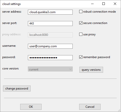
Client configuration
The configuration of the client, mainly regarding the cloud-service, is defined in the config.ini. While it can be directly edited, it is recommended to change it via the GUI settings. To save the password (using Windows Credential Manager), it needs to be entered once via the GUI settings. Note that the password has to be saved in order to run cloud simulations via the command-line. The default content of the config.ini is:
[cloud]
server address = cloud.quokka3.com
port number = 443
username = user@company.com
use secure connection = True
remember password = False
quokka3 core version = current
use proxy = False
proxy address = localhost:8080
robust connection mode = False
The “use secure connection” switch toggles between http (False) and https (True) protocol to be used for communication with the cloud. The default port is 80 for http and 443 for https.
If the “robust connection mode” switch is toggled, Quokka3 uses larger tolerances (timeouts and retries) for internet-connection, and a more stable way for transferring and updating logs. This should result in less “lost cloud connection” errors for low quality internet connections, at the expense of slower update frequency and responsiveness.
GUI
The purpose of the GUI is to conveniently control simulations and provide some basic results plotting functionality. It is not for defining the actual simulation parameters, which is done in the settingsfile. The plotting functionality provides a quick way to inspect main results, but it is not scoped to be a powerful generic post-processor. It’s up to the user to create any custom plots from the raw output data with his preferred tools.
Settings menu
Currently only some cloud settings are accessible via the settings menu, which will be read from and stored to the config.ini. Notably only the GUI is able to actually store the password (using Windows Credential Manager). Before being able to select a version, one must click “query versions” to list all versions available to the user. Note that it also sets the local version to be used.
Simulation tab
Here the simulation is controlled, i.e. you can essentially open a settingsfile, check the geometry, start the simulation and also cancel it if required. If you have signed up for a user account you can connect to the cloud, which will enable parallel mode, the option to disconnect a running cloud simulation and the possibility to manage cloud simulations. You may disconnect a running simulation and start more simulations simultaneously until the allowances set for your institution or group have been reached.
You can select a different solution type to override the setting in the settingsfile, to quickly simulate a variety of characteristics once your device properties are defined. If you enable the “append solution type to resultsfile name”, the name of the resultsfile will contain the solution type, which is useful to prevent accidently overwrites of the results.
In the “additional settings” text field you can enter any setting which will be added to or override the ones in the settingsfile. Multiple settings can be added by separating them via spaces. Therefore, any settings actually containing spaces need to be enclosed in double quotes, e.g:
"ContactFeature(1).Electrical.BarrierHeightType='from workfunction'" Solver.Sweep.Enable=0Checking “force storing spatial and map results” is identical to setting SaveSpatial and SaveMaps to 1.
It is good practice to always check geometry before starting simulations. This is a very quick sanity check, and even if connected to the cloud uses only the local executable for fast performance and robustness. Note that if you have a sweep defined, “check geometry” will disregard it. “check geometry” will run a simulation using the “meshing only” solution type and save the results in a filename including “meshing only”.
Manage cloud simulations dialog
In the top section the current usage and the allowances for the user-group you are associated with are shown. Usually, the group is your company or institute. This section is refreshed automatically.
In the bottom section, (only) your own simulations are listed, which are running, or not yet downloaded or deleted. You can double-click on a single simulation to open it, which will give a live log if still running or download results and delete it from the cloud if finished. You can select multiple simulations to delete directly.
Postprocessing tab
Once a simulation is finished in the simulation tab, it automatically switches to the postprocessing tab and loads the results file. Alternatively, a .h5 results file can be directly opened. There are 5 sub-tabs, which will be selectable only if the results contain respective data (see Output). E.g. the “Maps” tab can only be selected if the solution contains a map result.
Geometry tab
Here the geometry and mesh of the solution domain can be viewed if spatial results have been stored. It will render the plot into a Mayavi window, where you can rotate, zoom, move, save images etc. If one clicks check geometry, the geometry tab will be automatically selected and a plot will be created.
The button matrix toggles feature visibility for each plane. The buttons are disabled if no corresponding features are present on a plane. This is useful to sanity check the geometry definitions, and to spot inconsistencies. TO FAQ Note that occasionally some corners appear to be cut at an angle, which is purely a rendering artifact and not present in the actual simulation.
Note that a 2D geometry is still displayed as pseudo-3D. The size in y-coordinate is set arbitrarily for a sensible view, and only on a single side the 2D mesh exists.
1D geometry plotting is not yet supported.
Scalars (Sweep) tab
Here scalar results like efficiency can be plotted, but only if a sweep is defined (there is nothing to plot for a single point). The plot is created in a matplotlib window.
Curves tab
Here curves results like JV-curves can be plotted in various ways into a matplotlib window.
Maps tab
Here maps results like luminescence intensity map can be plotted into a matplotlib window.
Spatial tab
Here spatial results like band diagram or 2D cross sections can be plotted into a matplotlib window. Currently only plotting of 1D results is supported.
Matplotlib window
Most results are plotted into a matplotlib window, which provides some common scaling functionality. You can enter axis limits in the respective fields (empty for automatic) and press enter to apply. You can also toggle log-scales of the axis. You can save the plot in various formats for own further processing.
Updates
The GUI checks for updates each time you connect to the cloud. A popup windows will appear if an update is available, with the options to update now or later. Updating works completely automated and should be fast, as only differences are downloaded and applied (usually <10MB). A self-extracting archive (.exe) is executed during the update process, and you might get a respective warning.
If you want to keep the old version of Quokka3-client, simply duplicate the entire Quokka3 folder before updating.
Updating is strongly recommended as otherwise incompatibilities with the updated cloud-service can not be excluded.
Command-line
For scripted simulation control a command-line interface is provided via “Quokka3-cmd.bat”. The basic format to use it is
>Quokka3-cmd.bat [COMMAND] [PARAM1] [PARAM2]The return code is -1 on error, and unless otherwise stated 0 for success. Only the command START_LOCAL uses the local free version, all other commands control cloud simulations. They require correct client settings and the password to be stored.
START_LOCAL
Starts a local simulation, i.e. using the free Quokka3-core executable. PARAM1 is the settingsfile, PARAM2 is not used. Example:
>Quokka3-cmd.bat START_LOCAL "C:\my folder with spaces\mysettingsfile.m"START_WAIT
Starts a cloud simulation, continuously displays the log, downloads results and deletes the simulation from the cloud. PARAM1 is the settingsfile, PARAM2 is the number of cores to be used. Example:
>Quokka3-cmd.bat START_WAIT "C:\my folder with spaces\mysettingsfile.m" 2START_DISCONNECT
Starts a cloud simulation and immediately returns. PARAM1 is the settingsfile, PARAM2 is the number of cores to be used. The last output message is the SIMULATION ID, which is required for the GET_LOG and DOWNLOAD_RESULTS commands. Example:
>Quokka3-cmd.bat START_DISCONNECT "C:\my folder with spaces\mysettingsfile.m" 2GET_LOG
Retrieves and prints the log of a cloud simulation. Returns 0 if the simulation is finished, and 1 if it is still running. PARAM1 is the SIMULATION ID, PARAM2 is not used. Example:
>Quokka3-cmd.bat GET_LOG 1495811542680DOWNLOAD_RESULTS
Downloads results of a finished cloud simulation and deletes it from the cloud. PARAM1 is the SIMULATION ID, PARAM2 is not used. Example:
>Quokka3-cmd.bat DOWNLOAD_RESULTS 1495811542680Input (settingsfile)
Structure
All input parameters for the device properties and its characteristics to be simulated are defined in a settingsfile. It is a plain ASCII text file which can be edited by any text editor of your choice. While any extension is supported (e.g. .txt), it is recommended to use .m as the extension. It is noted however that the settingsfile is NOT interpreted as a Matlab-script, in particular no variables or mathematical expressions are supported. The *.m extension is solely useful to enable syntax highlighting in text-editors (e.g. Notepad++), as the settings syntax is derived from the Matlab syntax (mainly commenting via “%” and vector definition).
The settings consist of a list of assignments in the following exemplary form:
group.subgroup.parameter = value; % commentThere are four different types of values (no other types like variables or expressions are supported):
- switch: to enable or disable something by setting it to 1 or 0 respectively
- scalar: a single numeric value excluding any unit, which can be set in common formats (e.g. 110, 1.1e2 or 1.1E+02)
- string: a string value needs to be given in ‘single quotes’
- vector: a series of scalar values which can be defined in various ways
Some settings require the input of XY data points, e.g. for the generation profile. There is a common way to define such XY input data, including via loading it from a file.
Quokka3 supports various syntaxes for providing a generic way of defining the simulation setup (generic syntax), as well as simplified ways for various common simulation tasks (simplified syntaxes). With the considerably large functionality of Quokka3, the generic syntax unavoidably results in longish parameter names from nested groups. For an easier start simplified syntaxes are recommended, mainly simplifying geometry definitions, which as a compromise address only a subset of Quokka3 functionality.
The settings (except the high level settings) are organized into various levels of groups separated by a dot. In the following tables, the parameters need to be preceded by the respective name of the group. Default settings are marked with an Asterisk* and are not required to be given.
High level settings
| parameter | (recommended) value range | description |
|---|---|---|
| SaveSpatial | 1 / 0 | forces to save / not save spatial results; only applicable if the solution type has a unique operating point; Quokka3 decides based on mesh size etc. if not given |
| SaveMaps | 1 / 0 | forces to save / not save map results; only applicable if the solution type has a unique operating point; Quokka3 decides based on mesh size etc. if not given |
| DisplayPETSCResiduals | 1 / 0* | enables / disables printing of PETSC residuals (useful for checking convergence) |
| CoordinateOutputUnit | ‘m’, ‘cm’*, ‘mm’, ‘um’, ‘nm’ | sets the unit of coordinates in results file |
| Syntax | ‘generic’, ‘front and rear contact unit cell’, ‘1D detailed homojunction cell’, ‘near-surface skin’, ‘Quokka 2.2.5 FRC’ | What syntax to use: ‘generic’ for full functionality or simplified others for specific scenarios |
The parameters of the high level settings are applicable to all syntaxes.
Generic syntax
The ‘generic’ syntax is the fundamental way to define anything Quokka3 is capable of. The simplified syntaxes use parts of it.
Domain
Domain settings group:
| parameter (Domain) | (recommended) value range | description |
|---|---|---|
| .DeviceType | ‘semiconductor device’, ‘ohmic device’, ‘semiconductor skin’ | tells Quokka what kind of domain is to be modelled |
| .Dimensions | 1, 2, 3 | domain dimensions: 1D, 2D or 3D |
| .Wz | 0.1..200 \(\mu m\) | vertical domain size / device thickness (Z-coordinate); 1D, 2D and 3D; this is the thickness of the device’s bulk material excluding thin films and metal layers, i.e. the wafer thickness |
| .Wx | 1..2e5 \(\mu m\) | domain size in first lateral dimension (X-coordinate); 2D and 3D |
| .Wy | 1..2e5 \(\mu m\) | domain size in second lateral dimension (Y-coordinate); 3D only |
Solver
Solver settings group:
| parameter | (recommended) value range | description |
|---|---|---|
| .SolutionType | see next section | what device characteristic to simulate |
| .Illumination.Enable | 1 / 0 | only required if not implied by solution type |
| .Luminescence.Enable | 1 / 0 | defaults to 1 for ‘EL-PL’ solution type, and to 0 otherwise |
| .Electrical.MetalModelType | ‘constant-potential’, ‘finite-differences’ | 2D / 3D simulations only: ‘finite-differences’ includes metal layer in carrier transport modeling and requires definition of PadFeatures; ‘constant-potential’ sets the metal layer to uniform potential with the respective polarity (i.e. disables lateral current transport in metal) |
| .Electrical.NPMetalPadContact | ‘error’, ‘isolated’, ‘contact’ | defines the behavior for the case that a PadFeature covers a MetalFeatures with opposite polarity; ‘error’: gives error (default for a ‘semiconductor device’), ‘isolated’: assumes isolation, ‘contact’: allows current flow over the defined contact resistivity of the pad (default for an ‘ohmic device’) |
| .Electrical.MultiScaleQuality | 0.1..1*..10 | for multiscale modeling only: balances accuracy (higher value) against speed (lower value) for the coupling modes other than ‘single-point’ |
| .Electrical.VocGuess | 0.1..1.5 \(V\) | Voc guess, can help convergence and speed of some solution types |
| .Electrical.InitPrevious | 1* / 0 | whether to use a previous solution point to initialize the solution of the next point; speeds up various solution types; disabling can improve convergence in rare cases |
| .ExternalCircuit.Enable | 1 / 0* | whether to include external circuit elements |
| .Sweep.Enable | 1 / 0* | enables / disables parameter sweep |
| .IonModelType | ‘off’, ‘fixed’, ‘full’, ‘pre-bias’ | how to model ion transport; ‘pre-bias’ runs a separate simulation beforehand to find the steady-state ion concentrations defined by the Solver.IonPreBias group, and then fixes that ion concentration to simulate the conditions defined via Solver.SolutionType |
| .Timeout | 0*..1e4 \(s\) | maximum allowed computation time (per sweep point); set to 0 to disable (default); if this value is exceeded, an error is thrown; useful to set for sweeps where individual sweep points can become “stuck”: it allows the simulation to finish and to save the results of the other successfully solved sweep points |
The scope of the Solver group is to define the high-level options of the optical and electrical solvers Quokka3 employs. It also sets algorithms to iteratively apply or combine those solvers to simulate typical desired device characteristics. For example an automatic light JV-curve, which combines the optical and electrical solvers by an automatic algorithm to efficiently sweep the JV-curve.
Solver.SolutionType
The solution type defines what characteristic of the device to model, i.e. what kind of output to generate. There are different settings available for the different domain types:
- semiconductor device: ‘single JV-point’, ‘Tc light JV’ ‘dark JV-curve’, ‘light JV-curve’, ‘sunsVoc-curve’, ‘QE-curve’, ‘Rs-curve’, ‘Rs-MPP’, ‘EL-PL’ and ‘transient’
- semiconductor skin: ‘skin single-point’, ‘skin QE-curve’
- ohmic device: ‘Resistance’, ‘dark JV-curve’
- all domain types: ‘meshing only’
It is also mentioned whether the respective solution type contains a unique operating point, which decides whether any spatial or maps results can be present in the output files.
single JV-point
for domain type: ‘semiconductor device’; is a unique operating point
Solver.SingleJVPoint settings group:
| parameter | (recommended) value range | description |
|---|---|---|
| .Type | ‘Vintern’, ‘Vterm’, ‘Jterm’, ‘MPP’, ‘OC’, ‘Jsc’, ‘intrinsic’ | which operating point to (iteratively) simulate; ‘Vintern’ doesn’t require iterations and is thus faster than ‘Vterm’; ‘Jsc’ does NOT mean short-circuit, but a voltage somewhere between 0 \(V\) and \(V_{mpp}\) where the full \(J_{sc}\) is extracted (see Limits); ‘intrinsic’ means Vintern = 0V and no illumination |
| .Vintern | 0.1..2 \(V\) | internal voltage (excluding external circuit elements) for ‘Vintern’ type |
| .Vterm | 0.1..2 \(V\) | terminal voltage for ‘Vterm’ type |
| .Jterm | -1e3..1e3 \(mA/cm^2\) | terminal current for ‘Jterm’ type |
The ‘single JV-point’ solution type solves the device at a single operating point. Setting a fixed ‘Vintern’ is the fundamental way of solving a semiconductor device. The other types require iterations to a different degree, this being significantly slower than the ‘Vintern’ type.
Tc light JV
for domain type: ‘semiconductor device’; is a unique operating point
Solver.Tc settings group:
| parameter | (recommended) value range | description |
|---|---|---|
| .DeltaT | -10..10 \(K\) | temperature increment |
The ‘Tc light JV’ solution type simulates a light JV-curves both at the given and an incremental temperature, and calculates the temperature coefficients of the light JV parameters.
dark JV-curve and light JV-curve
for domain type: ‘semiconductor device’ and ‘ohmic device’ (dark JV-curve only); unique operating point for light JV-curve: MPP, none for dark JV-curve
Solver.JVCurve settings group:
| parameter | (recommended) value range | description |
|---|---|---|
| .VtermStepSize | ‘coarse’, ‘standard’, ‘fine’, ‘very fine’, ‘user’ | ‘user’ disables the automatic light JV-curve algorithm and sets user-defined points instead |
| .VtermUserSteps | vector \(V\) | vector of terminal voltage values for ‘user’ step size |
The ‘dark JV-curve’ solution type solves a JV-curve without illumination. It does not have a unique operating point.
For the ‘light JV-curve’ illumination is enabled. The algorithm starts by finding open circuit (\(V_{oc}\)), and then scans the JV-curve to lower voltages until no significant change in current is observed, i.e. \(J_{sc}\) conditions are reached. This is most commonly the case at voltages significantly above 0 \(V\), and thus avoids to solve the numerically challenging short-circuit operating point. The algorithm then iteratively finds the maximum power point. By this approach, using otherwise coarsely spaced JV-points, the automatic light JV-curve algorithm ensures high accuracy of \(V_{oc}\), \(J_{sc}\), efficiency and fill-factor with a minimal number of JV-points.
sunsVoc-curve
for domain type: ‘semiconductor device’; no unique operating point
Solver.SunsVocCurve settings group:
| parameter | (recommended) value range | description |
|---|---|---|
| .SunsStepSize | ‘pFF-only’, ‘standard’, ‘fine’, ‘very fine’, ‘user’ | ‘pff-only’ does not scan a full curve, but directly finds the pseudo fill-factor |
| .SunsUserSteps | vector | vector of suns values to solve suns-Voc curve at, for ‘user’ step size |
The ‘sunsVoc-curve’ solution type finds \(V_{oc}\) for a range of suns values.
QE-curve
for domain type: ‘semiconductor device’; no unique operating point
Solver.QECurve settings group:
| parameter | (recommended) value range | description |
|---|---|---|
| .Type | ‘biased’, ‘unbiased’ | ‘biased’ applies Optical.FrontIllumination and / or Optical.RearIllumination as bias illumination |
| .Side | ‘front’, ‘rear’ | from which side to apply the monochromatic illumination |
| .JgenMonochromatic | 0.1..10 \(mA/cm^2\) | monochromatic generation current density; additional for ‘biased’, total for ‘unbiased’ |
| .WavelengthStepSize | ‘coarse’, ‘standard’, ‘fine’, ‘very fine’, ‘user’ | predefined wavelength values, or ‘user’ |
| .WavelengthUserSteps | vector \(nm\) | user-defined vector of wavelength values |
The ‘QE-curve’ solution type simulates quantum efficiency of a ‘semiconductor device’. It requires spectrally resolved optical modeling, i.e. using the Text-Z model.
Rs-curve
for domain type: ‘semiconductor device’; unique operating point: MPP
Solver.RsCurve settings group:
| parameter | (recommended) value range | description |
|---|---|---|
| .Type | ‘DLM’, ‘dark-light-JV’, ‘sunsVoc-light-JV’ | which Rs calculation method to use |
The ‘Rs-curve’ solution type simulates an equivalent lumped series resistance Rs as a best fit to the IV-characteristics, for a range of terminal voltages. One can choose the method for Rs-extraction, you can find details in [???]. For the DLM method, a second illumination level at +0.5% is used. Note that different results can be expected for the different methods, in particular when bulk carrier transport (i.e. NON-series resistive effects) is significantly contributing to resistive losses.
Rs-MPP
for domain type: ‘semiconductor device’; unique operating point: MPP
There are no specific settings for this solution type.
The ‘Rs-MPP’ solution type simulates the equivalent lumped series resistance at maximum power point, using all of the methods of the Rs-curve setting, and additionally shows the value calculated from the integral of the resistive losses [FELA].
EL-PL
for domain type: ‘semiconductor device’; is a unique operating point
Solver.ELPL settings group:
| parameter | (recommended) value range | description |
|---|---|---|
| .Type | ‘PL’, ‘EL-Vterm’, ‘EL-Jterm’, ‘general-Vterm’, ‘general-Jterm’, ‘general-MPP’, ‘general-Jsc’ | what terminal condition to apply; ‘PL’ means open-circuit with illumination, ‘EL’-types mean without illumination, ‘general’-types mean user-defined illumination and terminal condition; ‘Vterm’-types apply a defined terminal voltage, ‘Jterm’-types a defined terminal current density, ‘MPP’ means maximum power point, ‘Jsc’ means \(J_{sc}\) condition (NOT short-circuit) |
| .Vterm | 0.1..2 \(V\) | terminal voltage for ‘Vterm’-types |
| .Jterm | -1e3..1e3 \(mA/cm^2\) | current density for ‘Jterm’-types |
The ‘EL-PL’ solution type simulates a luminescence map. It outputs a hyperspectral map, i.e. a spectrum for each element in the xy-plane, a intensity map, as well as the integral intensity. Note that lateral light smear, which might be very significant for textured devices and / or when not using short-pass filtering, is NOT considered (see quasi-1D optics in Limits).
Resistance
for domain type: ‘ohmic device’; is a unique operating point
‘Resistance’ is the only applicable solution type for an ohmic device. It will apply 1V as terminal voltage and calculate the current. The resulting resistance is independent of the applied voltage, due to the entire device being ohmic.
skin single-point and skin QE-curve
for domain type: ‘semiconductor skin’; is a unique operating point
Solver.Skin settings group:
| parameter | (recommended) value range | description |
|---|---|---|
| .iSkinFeature | 1.. | the index of the SkinFeature to be solved |
| .iContactFeauture | 0.. | the index of the ContactFeature to be applied to the skin (0 for non-contacted skin) |
| .iMetalFeauture | 0.. | the index of the [MetalFeature][MetF] to be applied to the skin (0 for no metal) |
| .QFPsplit | 0..2 \(V\) | quasi-Fermi potential split at the bulk-side boundary condition |
| .Jterm | -1e3..1e3 \(mA/cm^2\) | net current density through skin |
| .Resolution | 5..50 | number of points to be used each when varying above two parameters during presolving for multiscale modeling |
Uses the skin solver to simulate a skin - contact - metal combination and parameterize the results. ‘skin single-point’ performs one simulation for a single operating point. ‘skin QE-curve’ calculates the skin’s quantum efficiency, by first simulating the skin in the dark and then with illumination of different wavelengths. It uses the Solver.QECurve wavelength step setting to define the range of wavelengths.
transient
for domain type: ‘semiconductor device’; 1D with ‘fullsemicon’ bulk only; unique operating point: multiple snapshots
Solver.Transient settings group:
| parameter | (recommended) value range | description |
|---|---|---|
| .JVType | ‘Jintern’, ‘Vintern’ | whether a (transiently varying) terminal voltage or current density is applied; open circuit is defined by setting ‘Jintern’ and all zero .JVInput |
| .JVInput | XY input [\(\mu s\)], [\(V\) or \(mAcm^{-2}\)] | definition of the applied terminal voltage or current density over time |
| .GenerationScale | XY input [\(\mu s\)], [] | definition of the scaling factor for generation over time |
| .TimeSpan | 0..1e8 \(\mu s\) | total time to simulate |
| .SnapShotTimes | vector \(\mu s\) | NOT YET IMPLEMENTED; absolute time values on which to store spatial data |
| .SteadyStateSemiconductor | 1 / 0* | only applicable with ion transport: assumes (quasi-)steady-state electron and hole transport, which is valid if the concentrations equilibrate much faster than the time-scale of interest, and will result in much larger possible time steps and thus simulation speed |
| .SteadyStateTraps | 1 / 0* | assumes (quasi-)steady-state of general SRH recombination (trapping), which is valid if fundamental SRH lifetimes are much smaller than the time scale of interest, and will result in much larger possible time steps and thus simulation speed; this is NOT equivalent to simplified SRH, which additionally assumes a small trap density |
| .MaxTimeStep | 0..1e8 \(\mu s\) | sets an upper limit to the allowed time step |
| .MaxInitialTimeStep | 0..1 \(\mu s\) | the initial time step; default = 0.01 \(\mu s\) |
| .MaxChange | 0.01..0.4 | the maximum relative change of any property anywhere in the device within one time step; effectively sets a dynamic upper limit on the time step; default = 0.1 |
| .StartType | ‘standard’*, ‘intrinsic’ | Defines the steady-state conditions to be solved as a starting point; either using the t = 0 point of .JVInput and .GenerationScale (‘standard’, default), or intrinsic conditions (0 V and 0 generation); an ‘intrinsic’ is a robust way to replicate e.g. the transient behavior of an dark open-circuit device after switching the light on |
Performs a transient simulation using the 1D detailed solver. Two transiently varying properties can be defined: i) the terminal voltage or current density, ii) a scaling factor for illumination.
meshing only
for all domain types
‘meshing only’ does not run any simulation, but performs the meshing only. It is used by the “check geometry” functionality of the GUI.
Solver.Electrical.SkinJ0nieff
Solver.Electrical.SkinJ0nieff settings group:
| parameter | (recommended) value range | description |
|---|---|---|
| .Type | ‘user-T’, ‘user-const’ | how to set the value for \(n_{ieff}\) which was assumed when deriving \(J_{0}\) values; ‘user-T’ uses the material models for determining \(n_{ieff}\) for the given temperature |
| .T | 200..400 \(K\) | temperature assumed when deriving \(J_{0}\) values |
| .const | 8e9..1.5e10 \(cm^{-3}\) | \(n_{ieff}\) assumed when deriving \(J_{0}\) values |
The SkinJ0nieff group is required if one uses \(J_0\) inputs as a lumped skin recombination property. Because fundamentally not \(J_0\) but \(J_0/n_{ieff}^2\) can be considered constant, Quokka3 needs to know the \(n_{ieff}\) value which was assumed during the determination of \(J_0\). \(J_0\) can then be adjusted to be consistent with the \(n_{ieff}\) value of the simulation. For example, the “good old” spreadsheet of a Sinton lifetime tester does assume a constant value of 8.6e9 \(cm^{-3}\), whereas newer spreadsheets include a model for intrinsic carrier density and the same temperature as in the spreadsheet should be set here.
Solver.IonPreBias
Solver.IonPreBias settings group:
| parameter | (recommended) value range | description |
|---|---|---|
| .Type | ‘Vintern’, ‘Vterm’, ‘Jterm’, ‘MPP’, ‘OC’, ‘Jsc’, ‘pseudo-MPP’, ‘intrinsic’ | same as Solver.SingelJVPoint.Type |
| .Vintern | 0.1..2 \(V\) | internal voltage (excluding external circuit elements) for ‘Vintern’ type |
| .Vterm | 0.1..2 \(V\) | terminal voltage for ‘Vterm’ type |
| .Jterm | -1e3..1e3 \(mA/cm^2\) | terminal current for ‘Jterm’ type |
| .ScaleGeneration | 0..10 | optional parameter: overrides the scaling of the generation defined in Optical.ScaleGeneration (which is the default if not given) |
The ion pre-bias functionality will run two separate simulations:
- steady-state simulation to find the ion concentration profile for the conditions defined in this group
- subsequently applying the derived ion concentration as a fixed (immobile) concentration for the conditions defined in Solver.SolutionType
This is useful for example to conveniently replicate a fast JV-sweep after holding a cell pre-bias voltages. During the fast JV-sweep slow moving ions can be assumed to redistribute only marginally, i.e. showing a constant distribution, see this example.
Material
In the Material group the properties of all used materials are defined. It is separated into groups with the individual material’s short name.
Material.Si settings group for silicon properties:
| parameter | (recommended) value range | description |
|---|---|---|
| .AugerModel | ‘Si-Richter2012’*, ‘Si-Altermatt2011’, ‘Si-Sinton1987’ | Auger recombination model; note that only the Altermatt 2011 model includes temperature dependence |
| .BradModel | ‘Si-Nguyen’* | radiative recombination model |
| .DOSModel | ‘Si-Green1990’, ‘Si-Couderc2014’* | density of states model |
| .BandGapModel | ‘Paessler2002’* | band gap model |
| .ni0Model | ‘DOS-bandgap’*, ‘user-const’ | how to model intrinsic carrier density: either from DOS and band gap (default), or using a fixed user-defined value |
| .ni0 | 1e9..1e11 \(cm^{-3}\) | value for intrinsic carrier density for ‘user-const’ setting above |
| .BandGapMultiplier | ~1 | multiplies the band gap when calculating intrinsic carrier density from DOS and band gap; defaults to achieve \(n_{i0}=9.65e^9cm^{-3}\) at \(300K\) |
| .MobilityModel | ‘Si-Schindler2014’*, Si-Klaassen1992’, ‘user-const’ | mobility model, or user-defined constant mobilities |
| .HoleMobility | 10..10000 \(cm^2V^{-1}s^{-1}\) | mobility of holes for ‘user-const’ setting above |
| .ElectronMobility | 10..10000 \(cm^2V^{-1}s^{-1}\) | mobility of electrons for ‘user-const’ setting above |
| .BGNModel | ‘Si-Schenk1998’*, ‘Si-Schenk1998_LI’, ‘Si-Yan-Cuevas2014’, ‘off’ | band gap narrowing model; note that for the low-injection approximation of Schenk’s model, the parameterization given by Yan and Cuevas is used |
| .IncompleteIonizationModel | ‘off’*, ‘Si-Altermatt2006’ | incomplete ionization model |
| .PhosphorusLimit | ~2e20 \(cm^{-3}\) | maximum active doping concentration, concentration inputs above result in inactive phosphorus (solubility limit); defaults to a very high value, i.e. no limit |
| .BoronLimit | ~2e20 \(cm^{-3}\) | maximum active doping concentration, concentration inputs above result in inactive boron (solubility limit); defaults to a very high value, i.e. no limit |
| .nkModel | ‘user’, ’Si-Schinke2015-Green2008*’ | which model to use to define n&k values |
| .nk.n | XY input [\(nm\)], [] | wavelength-dependent real part of refractive index, for ‘user’ n&k |
| .nk.k | XY input [\(nm\)], [] | wavelength-dependent imaginary part of refractive index, for ‘user’ n&k |
Material.MAPbI3 settings group for MAPbI3 perovskite properties (default values from (???)]:
| parameter | (recommended) value range | description |
|---|---|---|
| .BandGap | 1.5* \(eV\) | band gap |
| .ElectronAffinity | 3.93* \(eV\) | electron affinity |
| .RelativePermittivity | 30* | relative permittivity |
| .HoleMobility | 2* \(cm^2V^{-1}s^{-1}\) | mobility of holes |
| .ElectronMobility | 2* \(cm^2V^{-1}s^{-1}\) | mobility of electrons |
| .Nc | 2.2e18* \(cm^{-3}\) | conduction band density of states |
| .Nv | 1.8e19* \(cm^{-3}\) | valence band density of states |
| .Brad | 6e-10* \(cm^3/s\) | radiative recombination coefficient |
| .Auger.Cn | 0* \(cm^6/s\) | (electron) Auger recombination coefficient |
| .Auger.Cp | 0* \(cm^6/s\) | (hole) Auger recombination coefficient |
| .CationMobility | 0..1e-9 \(cm^2V^{-1}s^{-1}\) | mobility of cations |
| .AnionMobility | 0..1e-9 \(cm^2V^{-1}s^{-1}\) | mobility of anions |
| .N0cat | 1e15..1e19 \(cm^{-3}\) | average cation concentration |
| .N0an | 1e15..1e19 \(cm^{-3}\) | average anion concentration |
| .nkModel | ‘user’, ’MAPbI3-Leguy2016*’ | which model to use to define n&k values |
| .nk.n | XY input [\(nm\)], [] | wavelength-dependent real part of refractive index, for ‘user’ n&k |
| .nk.k | XY input [\(nm\)], [] | wavelength-dependent imaginary part of refractive index, for ‘user’ n&k |
Optical
The optical group comprises the settings to define both illumination leading to generation, as well as luminescence of the device.
There is a common distinction on the locality of some settings indicated by the keywords global and local:
- global: the property is applied uniformly to the entire device.
- local: the property is defined locally via the optical properties of the SkinFeatures present at each lateral position.
General optical settings
Optical settings group:
| parameter | (recommended) value range | description |
|---|---|---|
| .GenerationModelType | ‘defined-generation’, ‘Text-Z’, ‘SunSolve’ | how to model generation, either by user-defined generation rate, or using the Text-Z model; if selecting ‘SunSolve’, ray-tracing results from the PV Lighthouse SunSolveTM can be easily imported to Quokka3 |
| .CorrectToKnownJgen | 1 / 0* | scales the generation profile to match a known generation current density; useful to correct for numerical errors (from interpolation and integration) |
| .Jgen | 10..100 \(mA/cm^2\) | generation current density used if above settings is enabled |
| .ScaleGeneration | 0.01..5 | scales the generation and the illumination intensity (for a correct efficiency); corresponds to “suns” if the generation was defined for 1 sun conditions |
Optical.DefinedGeneration
Optical.DefinedGeneration settings group:
| parameter | (recommended) value range | description |
|---|---|---|
| .Type | ‘uniform-G’, ‘uniform-Jgen’, ‘profile’ | how to set the defined generation |
| .UniformG | 1e17..1e20 \(cm^{-3}s^{-1}\) | uniform generation rate |
| .UniformJgen | 1..100 \(mA/cm^2\) | generation current density distributed uniformly over the device thickness |
| .Profile | XY input [\(\mu m\)], [\(cm^{-3}\) or \(cm^{-2}\)] | user generation profile; X-data means the closest distance to the illuminated surface; the unit of the Y-data depends on whether a standard or cumulative generation profile is used; |
| .Profile.Cumulative | 1 / 0 | whether the profile is cumulative (recommended for lower numerical error) or standard |
| .IlluminationIntensity | ~100 \(mW/cm^2\) | illumination intensity required for efficiency calculation; defaults to 100 \(mW/cm^2\); set to 0 if unknown; |
| .IlluminationSide | ‘front’*, ‘rear’ | which side of the device is illuminated; note that bifacial illumination is not supported for defined generation |
Optical.FrontIllumination / Optical.RearIllumination
Optical.FrontIllumination / Optical.RearIllumination settings group:
| parameter | (recommended) value range | description |
|---|---|---|
| .Enable | 1 / 0* | enable or disable illumination on the respective side |
| .Spectrum | XY input [\(nm\)], [\(mWcm^{-2}nm^{-1}\)] | user-defined spectrum |
| .Spectrum.Type | ‘AM1.5g’, ‘monochromatic’ | additional spectrum types instead of user-defined ones |
| .Spectrum.MonoWavelength | 200..2000 \(nm\) | wavelength for monochromatic illumination |
| .Spectrum.MonoFlux | 1e16..1e18 \(cm^{-2}s^{-1}\) | photon flux for monochromatic illumination |
| .Scale | 0.01..5 | scales the illumination, has the same effect as Optical.ScaleGeneration for monofacial illumination |
| .Shape | ‘full’*, ‘rectangle’ | illumination shape, defaults to full area |
| .PositionX | 0..2e5 \(\mu m\) | center position of non full area illumination |
| .PositionY | 0..2e5 \(\mu m\) | center position of non full area illumination |
| .SizeX | 0..2e5 \(\mu m\) | size of non full area illumination |
| .SizeY | 0..2e5 \(\mu m\) | size of non full area illumination |
The illumination settings are NOT applicable for the ‘defined-generation’ generation type and are ignored then. They are also used for a SunSolve file input when the ‘Text-Z’ input data are used.
Optical.TextZ
The “Text-Z” model is the recommended way to define the optics of the solar cell. It is superior to defining generation e.g. via a generation profile file, as the input parameters are (to good approximation) independent of i) the incident spectrum (which enables quantum efficiency simulations), ii) the device temperature and iii) if the parameterization of \(Z\) is used: the device thickness. The input parameters \(T_{ext}\) and \(Z\) can either be derived from spectral response and reflectance measurements, or from detailed optical simulations (e.g. a ray-tracer). See a more detailed description in the modelling guide.
Optical.TextZ.FrontText / Optical.TextZ.RearText settings group:
| parameter | (recommended) value range | description |
|---|---|---|
| .Type | ‘global-lumped’, ‘local-lumped’ | whether lumped front surface transmission is defined globally or for each SkinFeature |
| .Global | XY input [\(nm\)], [] | global definition of front surface transmission, must not include shading from metal and pad features |
| .Global.FacetAngle | 0..90° | characteristic facet angle of surface morphology for global definition |
The external transmission \(T_{ext}\) is the fraction of incident photons which reach the absorber, for front or rear side illumination. It is 1 - reflection (excluding escape reflection) - front film absorption.
Optical.TextZ.FrontZ / Optical.TextZ.RearZ settings group:
| parameter | (recommended) value range | description |
|---|---|---|
| .Type | ‘global-user’, ‘global-parameterization’, ‘global-4n2-limit’, ‘global-Green02-limit’, ‘local-lumped’ | how Z is defined; either globally for the entire device: via XY-input, a parameterization, the ideal \(4n^2\) limit, or a more realistic limit published in (Green 2002); or ‘local-lumped’ where Z is calculated locally from the internal optical properties of the SkinFeatures; see Modelling guide for more details and the this example |
| .Global | XY input [\(cm^{-1}\) or \(nm\)], [] | global user-defined Z |
| .Global.XType | ‘wavelength’, ‘absorption coefficient’ | whether X-data of XY input is the absorption coefficient (recommended) or wavelength |
| .Param.Z0 | 1..100 | Z parameter representing the low absorption limit (near band gap) |
| .Param.Zinf | 1..10 | Z parameter representing the high absorption limit |
| .Param.Zp | 1..10 | parameter influencing the trend between Z0 and Zinf |
The pathlength enhancement factor \(Z\) (as a function of absorption coefficient or wavelength) quantifies light trapping in the device. Generally it is different for front and rear illumination, that’s why \(Z\) needs to be differentiated to both cases.
Optical.SunSolve
Optical.SunSolve settings group:
| parameter | (recommended) value range | description |
|---|---|---|
| .File | ‘filename’ | SunSolveTM file, available via exporting to Quokka3 |
| .InputType | ‘Text-Z’, ‘generation-profile’ | enforce which kind of data to use; if not given, Quokka3 chooses automatically depending on availability of data |
If a SunSolve input is chosen, Quokka3 sets all relevant optical settings to match the results of a SunSolve simulation (an optical simulation software for solar cells and modules PV Lighthouse website). It is therefore the easiest way to interface Quokka3 with a ray-tracer, as error checks etc. are performed on the compatibility of the input data, and therefore the likelihood of mistakes and inconsistencies is minimized.
Note that currently the effect of metal shading is not interfaced but independently considered in both tools. Therefore the user must ensure that shading is not wrongly considered twice, i.e. on should set zero metal shading either in SunSolve or Quokka3 (in the latter case the spatial locality of the shading will not be considered, but generation is scaled down uniformly). Metal shading in Quokka3 is defined via the metal (and pad) geometry, and for each MetalFeature and PadFeature by the ‘.Optical.ShadingFraction’ parameter.
Generally, Quokka3 can use two different types of input data which may be contained in the SunSolve file, depending on what the simulation settings in SunSolve have been: Text-Z data (subsequently using the ‘Text-Z’ model to derive generation), or the generation-profile. Quokka3 will automatically choose the kind of input data based on availability and suitability, unless a specific type is enforced via ‘Optical.SunSolve.InputType’. The differences between the two types are detailed below:
- generation-profile:
- Gives highest accuracy of shape of generation profile :smiley:
- Works with any kind of (front-side only!) illumination: multiple light sources, isotropic illumination, angled illumination :smiley:
- Is specific to the illumination spectrum and temperature set in SunSolve, i.e. when changing those parameters separate SunSolve simulations and files are required; in particular it is not compatible with quantum-efficiency simulations :rage:
- Does (currently) only work for front illumination, i.e. not for rear / bifacial illumination :rage:
- Requires more ray tracing effort (simulation time) :rage:
- Text-Z:
- Input is independent of the illumination spectrum and temperature (and soon device thickness) set in SunSolve; a single SunSolve file is compatible with quantum-efficiency simulation, varying illumination spectrum and varying temperature :smiley:
- Works well for rear / bifacial illumination :smiley:
- Requires less ray tracing effort (simulation time) :smiley:
- Underlying simplifications may lead to inaccuracies in the shape of the derived generation profile; however, for typical silicon solar cells those inaccuracies have been shown to be negligible in (Fell, McIntosh, and Fong 2016) :neutral_face:
- does (currently) support only normal incidence illumination :rage:
Optical.Luminescence
Optical.Luminescence settings group:
| parameter | (recommended) value range | description |
|---|---|---|
| .Type | ‘local-lumped’ | only a local lumped model is supported yet: it uses the front surface transmission defined in the Text-Z model, and some additional internal reflectivities for each skin feature |
| .Scale | 0.. | simply scales the resulting luminescence signal; useful to calibrate to experimental units like counts / pixel |
| .OpticsAcceptanceAngle | 0..6.28 | solid acceptance angle of the detection optics (4pi = full sphere) |
| .OpticsTransmission | XY input [\(nm\)], [] | spectral transmission of the detection optics |
| .SensorEQE | XY input [\(nm\)], [] | spectral sensitivity (= external quantum efficiency) of detection sensor |
| .DetectionSide | ‘front’, ‘rear’ | on which side the luminescence signal should be detected |
| .WavelengthRange | vector \(nm\) | at which wavelength points to calculate luminescence |
| .GlobalMetalShadingFraction | 0..1* | internal shading fraction of Metal; defaults to 1, meaning that no signal is detected at metal features; useful to set to 0 if metal features only represent virtual or effective contacts |
| .EnableIdealEscape | 1 / 0* | enables ideal escape probability: no reabsorption and perfect rear reflection; default is off |
Bulk
| parameter | (recommended) value range | description |
|---|---|---|
| Bulk.Material | ‘Si’*, ‘MAPbI3’ | the material of the bulk, the qn-bulk solver supports currently only ‘Si’ |
| Bulk.Electrical.CarrierTransport | ‘quasineutral’*, ‘fullsemicon’ | only for a 1D ‘semiconductor device’: whether to use the qn-bulk solver or the 1D detailed solver for simulating bulk carrier transport |
| Bulk.Electrical.EnableIons | 1 / 0 | Enables ion transport in the bulk, only possible with the 1D detailed solver |
Bulk.Mesh
Bulk.Mesh settings group:
| parameter | (recommended) value range | description |
|---|---|---|
| .Quality | ‘coarse’*, ‘standard’, ‘fine’, ‘very-fine’, ‘user’ | how fine to discretize the geometry; note that the automatic meshing is scoped in such way that also a ‘coarse’ mesh will result in sufficient numerical accuracy in most cases, and is thus recommended; however, checking mesh-independency is the responsibility of the user |
| .dxmin | 0.1..10 \(\mu m\) | minimum lateral element size in x-direction (for ‘user’) |
| .dymin | 0.1..10 \(\mu m\) | minimum lateral element size in y-direction (for ‘user’) |
| .dzmin | 1e-2..10 \(\mu m\) | minimum vertical element size in z-direction (for ‘user’) |
| .dxmax | 1..1e4 \(\mu m\) | maximum lateral element size in x-direction (for ‘user’) |
| .dymax | 1..1e4 \(\mu m\) | maximum lateral element size in y-direction (for ‘user’) |
| .dzmax | 1..1e4 \(\mu m\) | maximum vertical element size in z-direction (for ‘user’) |
| .inflation | 1..4 | maximum allowed ratio in size of neighboring elements (for ‘user’) |
| .resolution | 3..30 | minimum amount of elements between any feature edges (for ‘user’) |
Bulk.Electrical.BackgroundDoping
Bulk.Electrical.BackgroundDoping settings group:
| parameter | (recommended) value range | description |
|---|---|---|
| .SettingType | ‘dopingtype-resistivity’, ‘NA-ND’ | whether doping is set via the doping type and a resistivity value, or directly via acceptor and donor concentrations |
| .DopingType | ‘n-type’, ‘p-type’ | for ‘dopingtype-resistivity’ |
| .Resistivity | 0.1..100 \(\Omega cm\) | for ‘dopingtype-resistivity’, and for ohmic simulations |
| .NA | 1..1e17 \(cm^{-3}\) | acceptor concentration for ‘NA-ND’ |
| .ND | 1..1e17 \(cm^{-3}\) | donor concentration for ‘NA-ND’ |
Bulk.Electrical.Recombination
Bulk.Electrical.Recombination settings group (also used by detailed skin properties):
| parameter | (recommended) value range | description |
|---|---|---|
| .Type | ‘off’, ‘intrinsic’, ‘intrinsic plus SRH’, ‘fixed-lifetime’, ‘intrinsic plus fixed-lifetime’, ‘lifetime-file’, ‘lifetime-curve’ | how to define recombination |
| .SRH(isrh).Type | ‘tau-Et’, ‘sigma-Et-Nt’, ‘sigma-Et-Nt-general’, ‘BO-Altermatt2011’, ‘Ph-precipitates’ | how to model SRH recombination; SRH settings are only applied for the ‘intrinsic plus SRH’ recombination type; the ‘sigma-Et-Nt-general’ type uses the general SRH formalism and can be set for a single defect and for 1D simulations only; all other types use the simplified SRH formalism |
| .SRH(isrh).Et_Ei | -1..1 \(eV\) | defect density relative to intrinsic energy (for ‘tau-Et’ and ‘sigma-Nt-Et’) |
| .SRH(isrh).taun | 1..1e5 \(\mu s\) | fundamental electron lifetime (for ‘tau-Et’) |
| .SRH(isrh).taup | 1..1e5 \(\mu s\) | fundamental hole lifetime (for ‘tau-Et’) |
| .SRH(isrh).Nt | 0..1e17 \(cm^{-3}\) | defect density (for ‘sigma-Nt-Et’) |
| .SRH(isrh).sigman | 1e-21..1e-15 \(cm^2\) | electron capture cross section (for ‘sigma-Nt-Et’) |
| .SRH(isrh).sigmap | 1e-21..1e-15 \(cm^2\) | hole capture cross section (for ‘sigma-Nt-Et’ or ‘Ph-precipitates’, default for the latter is 7.5e-18 \(cm^2\)) |
| .SRH(isrh).vth | 1e5..1e9 \(cm/s\) | OPTIONAL: thermal velocity (for ‘sigma-Nt-Et’); defaults to \(2e7\sqrt\frac{T}{300K}cm/s\) if not given |
| .SRH(isrh).BO_Oi | 0..1e17 \(cm^{-3}\) | oxygen concentration (for ‘BO-Altermatt2011’) |
| .SRH(isrh).BO_m | 1..3 | process related parameter scaling degraded lifetime (for ‘BO-Altermatt2011’) |
| .SRH(isrh).BO_DeactivationFraction | 0..1 | simply scales BO recombination (for ‘BO-Altermatt2011’) |
| .FixedLifetime | 1..1e5 \(\mu s\) | lifetime for ‘fixed-lifetime’ or ‘intrinsic plus fixed-lifetime’ recombination type |
| .LifetimeFile.Filename | ‘filename’ | name of .h5 file containing total bulk lifetime image(s); unit is \(\mu s\) INCLUDING intrinsic recombination; expects a 3D (Nx x Ny x Nimages) dataset named ‘Lifetime’ (for ‘lifetime-file’ recombination) |
| .LifetimeFile.PixelSize | 1..1e3 \(\mu m\) | size of the square area represented by one pixel of the image(s) (for ‘lifetime-file’ recombination) |
| .LifetimeFile.GenerationRate | vector \(cm^{-3}s^{-1}\) | generation rate for each image for multiple images (for ‘lifetime-file’ recombination) |
| .LifetimeFile.MinimumLifetime | ~1* \(\mu s\) | OPTIONAL this is the minimum local lifetime Quokka3 will apply when importing lifetime images; (very low local lifetime values can result in convergence problems) |
| .LifetimeCurve | XY input [\(cm^{-3}\)], [\(\mu s\)] | bulk lifetime as a function of excess carrier density INCLUDING intrinsic recombination, i.e. \(\tau_{bulk}(\Delta n)\) |
Multiple SRH defects can be defined simultaneously by consecutively increasing the index isrh starting at 1. Only a single SRH defect can be defined to use the general SRH formalism by using the ‘sigma-Et-Nt-general’ SRH type. A general SRH defect can be combined with the other (simplified) SRH types. The general SRH formalism is only supported within the 1D detailed solver, and can thus not be used for 2D / 3D simulations.
If lifetime images are loaded from a file, they will be centered to the solution domain. The user should ensure that the image covers the entire solution domain, otherwise some undefined extrapolation happens at the uncovered regions. If one image is defined, it represents an injection-independent lifetime map. For 2 images, Quokka3 calculates mid-gap \(\tau_{n0}\) and \(\tau_{p0}\) simplified SRH parameters for every pixel. For more images, the lifetime is found by spline-interpolation at the local injection level. Note that in each case intrinsic lifetime is treated separately: from the imported lifetime values intrinsic lifetime is subtracted (except for the case of a single image), and added again during the simulation. If multiple images do not span the required range of injection levels, extrapolation is performed by using the last (intrinsic lifetime corrected) value, i.e. a nearest neighbor extrapolation.
Features
Within the Quokka3 settings syntax, a feature means a homogeneous geometric region of either the skin-, metal- or pad-layer. Within each layer and on any side of the solution domain one can define multiple features, which are distinguished by an index in brackets, e.g. SkinFeature(1)., SkinFeature(2). and so on. The indices do not need to be consecutive, but the numbering is important, as for overlapping features within one layer the properties of the feature with the higher index will be assigned to that region. In short: for overlapping features, the highest index has priority.
E.g. to define a selective emitter structure, one would first define a full-area skin feature having the properties of the full-area emitter, and then define a line-shaped skin feature with a higher index having the properties of the selective emitter, which will override the first skin feature where present.
While not requiring consecutive numbering, within each type of feature the indices must be unique. E.g. each skin feature must have a unique index even though they might be on different sides of the solution domain, but both the skin features and contact features can start at index 1.
Common to all features is the “Name” parameter, which serves to differentiate the results like for example the loss breakdown.
| parameter | (recommended) value range | description |
|---|---|---|
| SkinFeature(iskin).Name, ContactFeauture(icont).Name, MetalFeature(imet).Name, PadFeature(ipad).Name | ‘feature name’ | name of the feature |
Feature Geometry
SkinFeature(iskin).Geometry / ContactFeauture(icont).Geometry / MetalFeature(imet).Geometry / PadFeature(ipad).Geometry settings group:
| parameter | (recommended) value range | description |
|---|---|---|
| .Plane | ‘front’, ‘rear’, ‘west’, ‘east’, ‘north’, ‘south’ | which side the feature is placed on; pad features can only be at the front and rear side |
| .Shape | ‘full’, ‘rectangle’, ‘circle’ | feature shape; instead of using ‘circular’ it is recommended to use a square shape with equal area |
| .Inverse | 0* / 1 | If set to 1, the feature covers the full area except of the defined geometry; useful e.g. to create “gaps” |
| .PositionX | 0..2e5 \(\mu m\) | x-coordinate center position (for ‘front’, ‘rear’, ‘north’ and ‘south’ side only) |
| .PositionY | 0..2e5 \(\mu m\) | y-coordinate center position (for ‘front’, ‘rear’, ‘east’ and ‘west’ side only) |
| .PositionZ | 0..2e5 \(\mu m\) | z-coordinate center position (for ‘north’, ‘south’, ‘east’ and ‘west’ side only) |
| .SizeX | 0..2e5 \(\mu m\) | x-coordinate size (for ‘front’, ‘rear’, ‘north’ and ‘south’ side only) |
| .SizeY | 0..2e5 \(\mu m\) | y-coordinate size (for ‘front’, ‘rear’, ‘east’ and ‘west’ side only) |
| .SizeY | 0..2e5 \(\mu m\) | z-coordinate size (for ‘north’, ‘south’, ‘east’ and ‘west’ side only) |
| .RepetitionsX | 1*..1000 | number of identical features pitched in x-direction |
| .RepetitionsY | 1*..1000 | number of identical features pitched in y-direction |
| .RepetitionsZ | 1*..1000 | number of identical features pitched in z-direction |
| .PitchX | 0..2e5 \(\mu m\) | x-coordinate pitch (for ‘front’, ‘rear’, ‘north’ and ‘south’ side only) |
| .PitchY | 0..2e5 \(\mu m\) | y-coordinate pitch (for ‘front’, ‘rear’, ‘east’ and ‘west’ side only) |
| .PitchZ | 0..2e5 \(\mu m\) | z-coordinate pitch (for ‘north’, ‘south’, ‘east’ and ‘west’ side only) |
SkinFeature
SkinFeature(iskin).Geometry settings group additional to the general Feature Geometry group:
| parameter | (recommended) value range | description |
|---|---|---|
| .DepthType | ‘auto’*, ‘user’ | how to determine the skin depth, default and recommended setting is ‘auto’ |
| .DepthUser | 0..10 \(\mu m\) | user-defined skin depth, if above is set to ‘user’ |
Skin features have an additional geometric setting, which is the depth. The skin depth is not necessarily the thickness of the skin, but only the near-surface part. E.g. for a diffused surface the skin depth and skin thickness would be identical, while for a multilayer heterojunction skin the skin depth would only be the distance between the quasi-neutral bulk boundary and the Si - aSi interface. In most cases it should be best to use the “automatic” skin depth setting. If defined by the user, the user must ensure that the skin depth actually reaches into the quasi-neutral bulk. One case the user has to define the skin depth is when a lumped collection efficiency is set, as then Quokka3 needs to figure out the generation within the skin. It’s then up to the user to ensure consistency of optical generation, skin depth and collection efficiency.
Also a skin feature may be contacted or not. As the presence of a contact often changes the properties of the skin, like for example its recombination, some of the following settings are split into contacted and non-contacted.
SkinFeature(iskin) settings group:
| parameter | (recommended) value range | description |
|---|---|---|
| .ElectricalModelType | ‘lumped’, ‘detailed’ | whether to model the skin by lumped inputs or detailed inputs, the latter using the multiscale approach for a semiconductor device; ‘detailed’ is only supported for front and rear side skins |
| .OpticalModelType | ‘lumped’ | currently only lumped optical modeling is supported |
Lumped.Optical
SkinFeature(iskin).Lumped.Optical settings group:
| parameter | (recommended) value range | description |
|---|---|---|
| .Text | XY input [\(nm\)], [] | front surface transmission |
| .FacetAngle | 0..90° | characteristic facet angle of surface morphology |
| .Internal.AverageReflectance | 0..1 | average internal reflectance |
| .Internal.SpecularReflectance | 0..1 | specular internal reflectance; optional parameter applicable to the illuminated side / luminescence detection side only, which otherwise defaults to the average internal reflectance; can be used to replicate the model inputs of (Brendel et al. 1996), where for a random texture with antireflection coating a specular reflectance of 0.62 and an average reflectance of 0.93 was determined |
| .Internal.LambertianFraction | 0..1 | Lambertian fraction, i.e. effective amount of scattering; applicable only for the side opposite to the illumination side / luminescence detection side |
The lumped optical properties of a skin are only applicable if they are required by a local optical modeling approach. The internal optical properties are used for luminescence modeling and for calculating local Z values.
The lumped optical parameters do not distinguish between the contacted and non-contacted regions of the skin. To be able to account for the optical differences, one must define two separate SkinFeatures for the contacted and non-contacted regions respectively.
Lumped.Electrical
SkinFeature(iskin).Lumped.Electrical settings group:
| parameter | (recommended) value range | description |
|---|---|---|
| .RsheetEnable | 1 / 0 | enable / disable lateral conductance |
| .Rsheet | 1e-3..1e5 \(\Omega\) | sheet resistance, if enabled above |
| .ConductionType | ‘n-type’, ‘p-type’ | which type of carriers are transported within skin, only required if sheet resistance is enabled |
| .ContactedRecombination / .NonContactedRecombination | settings groups for skin recombination properties (see below) | |
| .VerticalResistivity | OPTIONAL vertical resistivity settings group (see below) | |
| .EtaColl | XY input [\(nm\)], [\(cm^{-1}\)] | OPTIONAL collection efficiency as a function absorption coefficient; is assumed 1 when not defined; requires a user-defined skin depth if set |
| .WestEdgeJ02, .EastEdgeJ02, .NorthEdgeJ02, .SouthEdgeJ02 | 0*..19e-9 \(A/cm\) | OPTIONAL for front and rear side skins only: represents recombination at a space-charge-region bordering at the respective edge by an edge-length specific \(J_{02,edge}\); the skin must be of opposite doping type to the bulk, i.e. must form a pn-junction; 19 \(nA/cm\) represents a general worst-case value for a clean edge without any passivation effect; see details of the model in (Fell et al. 2018) |
SkinFeature(iskin).Lumped.Electrical.VerticalResistivity settings group:
| parameter | (recommended) value range | description |
|---|---|---|
| .Enable | 1 / 0* | enable / disable a vertical resistivity between the bulk and the skin |
| .Type | ‘ohmic’, ‘MIS_simple’ | type of vertical resistivity: a constant ‘ohmic’ value, or a non-ohmic ‘MIS_simple’ model (see also explanations at ContactFeauture) |
| .SchottkyBarrier | -1..5 \(eV\) | Schottky barrier height (for ‘MIS_simple’) |
| .TunnelBarrier | 0..5 \(eV\) | barrier height of tunneling (insulator) layer (for ‘MIS_simple’) |
| .TunnelThickness | 0..10 \(nm\) | thickness of tunneling (insulator) layer (for ‘MIS_simple’) |
| .EffectiveMass | 0.01..1*..2 | effective tunneling mass, fraction of electron rest mass; defaults to 1 (for ‘MIS_simple’) |
| .OhmicResistivity | 0..1..1e10 \(\Omega cm^2\) | ohmic contact resistivity; for ‘MIS_simple’ this resistivity is placed in parallel to the MIS current transport |
SkinFeature(iskin).Lumped.Electrical.ContactedRecombination / SkinFeature(iskin).Lumped.Electrical.NonContactedRecombination settings groups:
| parameter | (recommended) value range | description |
|---|---|---|
| .ModelType | ‘J0’, ‘Seff’, ‘J0(V)’, ‘Seff(deltan)’, ‘off’ | how to model recombination |
| .J0 | 1e-16..1e11 \(A/cm^2\) | \(J_{0,skin}\), requires to define the intrinsic carrier density which was assumed when deriving this value |
| .Seff | 0..1e6 (..1e7) \(cm/s\) | effective surface recombination velocity; 1e7 might sometimes lead to convergence issues, use max. 1e6 which is usually well high enough |
| .J0(V) | XY input [\(V\)], [\(A/cm^2\)] | defines \(J_{0,skin}\) as a function of the bulk-side quasi-Fermi level split; note that this corresponds often, but not generally, to the voltage of the device |
| .Seff(deltan) | XY input [\(cm^{-3}\)], [\(cm/s\)] | defines \(S_{eff}\) as a function of bulk-side excess carrier density |
Detailed: Mesh
SkinFeature(iskin).Detailed.Mesh settings group:
| parameter | (recommended) value range | description |
|---|---|---|
| .Quality | ‘coarse’, ‘standard’, ‘fine’, ‘very-fine’, ‘user’ | how fine to discretize the geometry; for the 1D detailed solver ‘standard’ is recommended and should be sufficiently accurate in most cases; however, checking mesh-independency is the responsibility of the user |
| .dzmin | 1e-3..0.1 \(\mu m\) | minimum element size (for ‘user’) |
| .dzmax | 1e-2..10 \(\mu m\) | maximum element size (for ‘user’) |
| .inflation | 1..4 | maximum allowed ratio in size of neighboring elements (for ‘user’) |
| .resolution | 3..30 | minimum amount of elements for any layer (for ‘user’) |
Detailed: Layers
SkinFeature(iskin).Detailed.Layer(ilay) settings group:
| parameter | (recommended) value range | description |
|---|---|---|
| .Name | ‘name’ | name of layer |
| .Type | ‘near-surface’ | ‘near-surface’ means that the layer is part of the bulk material without any bulk-side interface physics, i.e. using a quasi-neutral boundary condition. The first layer of a skin must always be a near-surface type. Currently this is the only supported option. |
A skin consists of several layers which must be consecutively indexed. Currently only a single layer with near-surface type is supported.
Detailed: DopingProfiles
SkinFeature(iskin).Detailed.Electrical.Layer(ilay).DopingProfile / SkinFeature(iskin).Detailed.Electrical.Layer(ilay).ActiveProfile settings group:
| parameter | (recommended) value range | description |
|---|---|---|
| XY input [\(\mu m\)], [\(cm^{-3}\)] | The DopingProfile and optional ActiveProfile groups are XY-inputs to define doping profiles additional to the background doping with some extended options below | |
| .Type | ‘off’*, ‘box’, ‘gauss’, ‘erfc’ | types to define the shape of the profile additional to the common XY input types; defaults to ‘off’ which disables the profile |
| .DopingType | ‘p-type’, ‘n-type’ | doping type; for ‘none’, or if this parameter is not given, the entire settings group is disregarded |
| .Npeak | 1e16..1e22 \(cm^{-3}\) | peak concentration for ‘box’, ‘gauss’, ‘erfc’ |
| .Depth | 0.1..10 \(\mu m\) | depth / depth factor for ‘box’, ‘gauss’, ‘erfc’ |
| .Offset | 1e-3..1 \(\mu m\) | distance between outer interface of layer and peak concentration for ‘gauss’, ‘erfc’ |
The DopingProfile is the total doping concentration. The ActiveProfile is optional. If both are defined, the difference results in inactive dopants and other incomplete ionization models are disregarded. If only the DopingProfile is defined, inactive dopants are calculated via the incomplete ionization models. One can not set an ActiveProfile only, rather set the DopingProfile only and switch off incomplete ionization model.
The zero-point of the doping profiles, \(z_p=0\), are defined as the outward interface of the layer, which is not necessarily the surface for multilayer skins.
The definition for ‘gauss’ and ‘erfc’ profiles are the following:
- ‘gauss’: \(N_{dop}=N_{peak}exp(-{(z_p-offset)^2}/depth^2))\)
- ‘erfc’: \(N_{dop}=N_{peak}erfc((z_p-offset)/depth)\).
Detailed: Interface
for multiple layers only, not yet supported
Detailed: Surface
SkinFeature(iskin).Detailed.Electrical.ContactedSurface / SkinFeature(iskin).Detailed.Electrical.NonContactedSurface settings group:
| parameter | (recommended) value range | description |
|---|---|---|
| .RecombinationModel | ‘S’, ‘Dit-sigma’, ‘Si-SiO2-Altermatt2002’, ‘Si-SiNx-Min2014’, ‘Si-Kimmerle2016’ | how surface recombination is modeled; either using fundamental electron and hole surface recombination velocity inputs for surface SRH (‘S’), Dit and capture cross sections, or by using an empirical parameterization for Sn and Sp |
| .Kimmerle2016.Charge | 1 / 0* | 1: explicitly accounting for charge; 0: Sp and Sn include the effect of charge (‘Si-Kimmerle2016’ only) |
| .Kimmerle2016.Texture | 1 / 0 | whether to assume textured (1) or planar (0) surface (‘Si-Kimmerle2016’ only) |
| .Kimmerle2016.Stack | ‘SiOxNy-SiNx’, ‘SiO2-SiNx’ | which dielectric stack to assume (‘Si-Kimmerle2016’ only) |
| .Sn | 0..1e7 \(cm/s\) | fundamental electron surface recombination velocity (for ‘S’ model) |
| .Sp | 0..1e7 \(cm/s\) | fundamental hole surface recombination velocity (for ‘S’ model) |
| .Et_Ei | -1..1 \(eV\) | defect energy relative to intrinsic energy (for ‘S’ and ‘Dit-sigma’) |
| .sigman | 1e-20..1e-10 \(cm^2\) | electron capture cross section (for ‘Dit-sigma’) |
| .sigmap | 1e-20..1e-10 \(cm^2\) | hole capture cross section (for ‘Dit-sigma’) |
| .Dit | 0..1e20 \(cm^{-2}\) | surface defect density (for ‘Dit-sigma’) |
| .vth | 1e5..1e9 \(cm/s\) | OPTIONAL: thermal velocity (for ‘Dit-sigma’); defaults to \(2e7\sqrt\frac{T}{300K}cm/s\) if not given |
| .Charge | -1e13..0*..1e13 \(cm^{-2}\) | surface charge density, defaults to 0; ignored for contacted surface |
These groups define the recombination properties at the actual surface, or at the contact to the metal.
Detailed: Multiscale Modeling
SkinFeature(iskin).Detailed.Electrical.Multiscale settings group additional settings:
| parameter | (recommended) value range | description |
|---|---|---|
| .ModelType | ‘single point’, ‘injection dependent recombination’, ‘full coupling’ | see text below |
| .TextureMultiplierContacted | 1..2 | scales bulk-side recombination within multiscale modeling to account for higher recombination of a textured surface compared to the planar simulation; |
| .TextureMultiplierNonContacted | 1..2 | same as above for non-contacted skin region |
| .AddRsheetEnable | 1 / 0* | whether to consider an additional laterally conductive layer on top within this skin (e.g. a TCO) |
| .AddRsheet | 10..5000 \(\Omega\) | additional sheet resistance, if enabled above |
These settings are applicable if multiscale modeling is used, i.e. if this skin feature is defined by detailed inputs within a 2D or 3D semiconductor device (or within a 1D device using quasi-neutral bulk carrier transport).
There are three different types of coupling:
- ‘single point’: simulates and parameterizes the skin once at a single operating point (at the Voc guess and a small net current density), and assumes the parameters to be constant. This is fastest and most robust, and is well valid e.g. for highly doped near-surfaces like surface diffusions, which usually have a constant \(J_{0,skin}\) and a negligible vertical resistivity.
- ‘injection dependent recombination’: simulates and parameterizes the skin for a range of bulk-side Fermi-level splits and a at constant (and low) net current density. This is useful e.g. for lowly-doped surfaces passivated by a layer with moderate charge, which can show significant injection dependence of the recombination, but where vertical resistance is not relevant.
- ‘full coupling’: simulates and parameterizes the skin for all relevant operating points. This is the generally valid and thus the most accurate option, but at the expense of simulation time (significant for small to medium bulk mesh sizes).
The quality of ‘injection dependent recombination’ and ‘full coupling’ can be set by Electrical.Solver.MultiScaleQuality, which influences how finely the the Fermi-level split (and current density) is discretized, and thus balances accuracy against speed.
The texture multiplier scales bulk-side recombination, i.e. the \(J_{0,skin}\), within the multiscale modeling to account for the higher recombination of a textured surface compared to the planar simulation. Note that it does not influence the skin’s collection efficiency (as unavoidable for texture multipliers in fully detailed modeling).
ContactFeature
The geometry of a contact feature is set via the ContactFeature(icont).Geometry group which is identical to the Feature Geometry group.
ContactFeature(icont) settings group additional settings:
| parameter | (recommended) value range | description |
|---|---|---|
| .OhmicResistivity | 1e-6..1 \(\Omega cm^2\) | contact resistivity; for a contact to a lumped skin using the ‘MIS_simple’ model this value is applied in parallel to the MIS transport, e.g. representing pinholes; within multiscale modeling, this value is applied additionally (in series) to the contact resistivity extracted by the skin solver; for a 1D detailed cell simulation this value is disregarded (here one must define the contact resistivity as an external series resistance instead) |
| .CurrentTransportModel | ‘ohmic’, ideal’, ‘MIS_simple’, ‘MS’, ‘MIS’ | how to model current transport, see description below; defaults to ‘ideal’ for a detailed skin, and to ‘ohmic’ for a lumped skin |
The applicable settings for a ContactFeature depends on whether it is placed on a lumped or detailed skin. The options for a contact to a lumped skin are:
- ‘ohmic’ (default): simply applies an ohmic contact resistivity
- ‘MIS_simple’: uses a simplified MIS model resulting in a non-ohmic resistivity. It’s simplified compared to the ‘MIS’ option available for a contact to a detailed skin by i) neglecting the potential drop over the insulator and ii) not allowing to set current transport for minority carriers to non-zero. It is not possible to use the full ‘MIS’ model for current transport at lumped skins.
ContactFeature(icont) settings group additional settings for ‘MIS_simple’ current transport model (contact to a lumped skin):
| parameter | (recommended) value range | description |
|---|---|---|
| .SchottkyBarrier | -1..5 \(eV\) | Schottky barrier height (for ‘MIS_simple’) |
| .TunnelBarrier | 0..5 \(eV\) | barrier height of tunneling (insulator) layer |
| .TunnelThickness | 0..10 \(nm\) | thickness of tunneling (insulator) layer |
| .EffectiveMass | 0.01..1*..2 | effective tunneling mass, fraction of electron rest mass; defaults to 1 |
The options for a contact to a detailed skin are:
- ‘ideal’: assumes flat-band conditions, a negligible contact resistivity for majority carriers, and zero current extraction for minority carriers
- ‘MS’: Schottky-type contact
- ‘MIS’: extends ‘MS’ by accounting for a thin insulator layer via an analytical direct tunneling model
ContactFeature(icont) settings group additional settings for ‘MS’ and ‘MIS’ current transport model (contact to a detailed skin):
| parameter | (recommended) value range | description |
|---|---|---|
| .BarrierHeightType | ‘user’, ‘from workfunction’ | how to set the Schottky barrier height; either user-defined or calculated from metal workfunction and electron affinity of the skin (i.e. its outer layer’s material) |
| .BarrierHeightUser | -1..1 \(eV\) | user-defined barrier height |
| .Tunnel.Thickness | 0.1..10 \(nm\) | thickness of insulator layer, i.e. of rectangular tunneling barrier |
| .Tunnel.RelPermittivity | 1..1000 | relative permittivity of insulator layer |
| .Tunnel.ElectronBarrier | 0*..5 \(eV\) | tunneling barrier height for electrons |
| .Tunnel.HoleBarrier | 0*..5 \(eV\) | tunneling barrier height for holes |
| .Tunnel.ElectronEffectiveMass | ~1* | effective mass of electrons (relative to electron rest mass) |
| .Tunnel.HoleEffectiveMass | ~1* | effective mass of holes (relative to electron rest mass) |
| .OhmicElectronResistivity | 1e-6..1 \(\Omega cm^2\) | (optional) ohmic contact electron resistivity parallel to MS / MIS current transport; can be used to describe mixed tunnel and ohmic contacts (e.g. pinholes in tunnel oxide) |
| .OhmicHoleResistivity | 1e-6..1 \(\Omega cm^2\) | (optional) ohmic contact hole resistivity parallel to MS / MIS current transport; can be used to describe mixed tunnel and ohmic contacts (e.g. pinholes in tunnel oxide) |
| .ElectronBarrierOffset | -1..1 \(eV\) | (optional) offsets the electron barrier height for thermionic emission; can be used to account for a semiconductor buffer layer shifting the transport-limiting barrier to the metal - buffer layer interface |
| .HoleBarrierOffset | -1..1 \(eV\) | (optional) offsets the hole barrier height for thermionic emission; can be used to account for a semiconductor buffer layer shifting the transport-limiting barrier to the metal - buffer layer interface |
| .MinorityThermionicEmission | 1 / 0* | allow thermionic emission of minority carriers; defaults to off, which provides a more effective description of e.g. passivating contacts; needs to be enabled to account for selectivity losses caused by not very asymmetric barrier heights for electrons and holes |
Refer to the Modeling guide for details on the contact physics.
MetalFeature
The geometry of a metal feature is set via the MetalFeature(imet).Geometry group which is identical to the Feature Geometry group.
MetalFeature(imet) settings group additional settings:
| parameter | (recommended) value range | description |
|---|---|---|
| .Electrical.Polarity | ‘n-type’, ‘p-type’ | while there is obviously no ‘n-type’ or ‘p-type’ current transport in a metal, it is still important to define the (initial) polarity of the metal, i.e. to which polarity of the applied potential it is connected to. It defines whether a electron or hole contact model is applied to a contacted detailed skin. Also it is required for Quokka3 to find sensible start values. |
| .Electrical.Rsheet | 1e-3..1 \(\Omega\) | sheet resistance of the metal, only applicable if the metal is solved by finite differences |
| .Electrical.WorkFunction | 0..10 \(eV\) | only used for a Schottky-type contact where the barrier height is derived from the workfunctions |
| .Optical.ShadingFraction | 0..1* | shading fraction of the metal feature to account for reflected and scattered light still contributing to generation |
PadFeature
Pad features are only required if the metal is solved by finite differences, otherwise the settings will be ignored.
The geometry of a pad feature is set via the PadFeature(ipad).Geometry group which is identical to the Feature Geometry group.
PadFeature(ipad) settings group additional setting:
| parameter | (recommended) value range | description |
|---|---|---|
| .Electrical.Polarity | ‘n-type’, ‘p-type’ | defines the polarity of the applied potential |
| .Electrical.ContactResistivity | 1e-6..1 \(\Omega cm^2\) | contact resistivity between pad and metal |
| .Optical.ShadingFraction | 0..1 | shading fraction of the pad feature to account for reflected and scattered light still contributing to generation |
ExternalCircuit
External circuit elements are accounted for one when enabled in the Solver group. Then the terminal voltage is different to the voltage applied to the device, which is the internal voltage.
ExternalCircuit settings group:
| parameter | (recommended) value range | description |
|---|---|---|
| .Rseries | 0..10 \(\Omega cm^2\) | series resistance |
| .Rshunt | 1e2..1e10 \(\Omega cm^2\) | shunt resistance |
| .DiodeJ0 | 0..1e-5 \(A/cm^2\) | diode saturation current density |
| .DiodeIdeality | 1..3 | ideality factor of diode |
Probes
Probes have the purpose to define a position within the solution domain where to probe a specific solution quantitiy. They do not influence the simulation result in any form. For example, probes can be defined to represent voltage sense probes within a four-point-probe setup.
Currently, only surface voltage probes are supported, representing physical probes being placed on the outer surfaces of the device. Such a probe will sense either the voltage of the skin layer at the defined position, or of the metal layer in case a metal feature is present.
Probe(iprobe) settings group:
| parameter | (recommended) value range | description |
|---|---|---|
| .Name | ‘probe name’ | name of probe |
| .Plane | ‘front’, ‘rear’, ‘west’, ‘east’, ‘north’, ‘south’ | which side the probe is placed on |
| .PositionX | 0..2e5 \(\mu m\) | x-coordinate center position (for ‘front’, ‘rear’, ‘north’ and ‘south’ side only) |
| .PositionY | 0..2e5 \(\mu m\) | y-coordinate center position (for ‘front’, ‘rear’, ‘east’ and ‘west’ side only) |
| .PositionZ | 0..2e5 \(\mu m\) | z-coordinate center position (for ‘north’, ‘south’, ‘east’ and ‘west’ side only) |
Sweep
A sweep, if enabled in the Solver group, varies input parameters for a series of defined values. It supports two independent sweep groups A and B, within each multiple parameters can be varied at the same time. Within each group, the number of sweep values must be equal for all parameters. That means that (up to) a 2-dimensional sweep can be defined, where each dimension can consist of multiple simultaneously varied parameters. If a higher dimensional sweep it desired it is up to the user to linearize it into a 2- or 1-dimensional sweep.
Currently the performance of the sweep is the same as when those simulations would be started individually. However there are some advantages of doing the sweep within Quokka3:
- gives a single results file summarizing all sweep results
- plotting functionality of GUI has the capability of quickly plotting main results as a function of the sweep parameters
- can be run in parallel mode to solve sweep points simultaneously
- In future, performance will be better in certain scenarios, as Quokka3 can re-use some results from previous sweep-points for a faster simulation
Sweep settings group:
| parameter | (recommended) value range | description |
|---|---|---|
| .NGroups | 1 / 2 | number if independent sweep groups; 1 means group A only, 2 means group A and B |
| .GroupA(ia).Parameter | ‘parameter name’ | can be any input parameter which sets a scalar value; sweeping of other types like string parameters is not supported; multiple, consecutively indexed parameters can be defined |
| .GroupA(ia).Values | vector | vector of values; the same unit as for the respective parameter applied; all vector values within a group must have the same length |
| .GroupB(ib).Parameter | ‘parameter name’ | same as for GroupA |
| .GroupB(ib).Values | vector | same as for GroupB |
As an example, the sweep settings
Solver.Sweep.Enable = 1; % enable sweep
Sweep.NGroups = 2;
Sweep.GroupA(1).Parameter = 'SkinFeature(1).Lumped.Electrical.Rsheet';
Sweep.GroupA(1).Values = [70 100 150];
Sweep.GroupA(2).Parameter = 'SkinFeature(1).Lumped.Electrical.J0'; % dependent parameter: higher Rsheet means lower J0
Sweep.GroupA(2).Values = [150 100 70]*1e-15;
Sweep.GroupB(1).Parameter = 'Bulk.Electrical.BackgroundDoping.Resistivity'; % independent parameter
Sweep.GroupB(1).Values = [2 3];
will simulate the following 6 sweep points (shown in linearized form):
| # | ia | ib | Rsheet | J0 | Resistivity |
|---|---|---|---|---|---|
| 1 | 1 | 1 | 70 | 150e-15 | 2 |
| 2 | 1 | 2 | 70 | 150e-15 | 3 |
| 3 | 2 | 1 | 100 | 100e-15 | 2 |
| 4 | 2 | 2 | 100 | 100e-15 | 3 |
| 5 | 3 | 1 | 150 | 70e-15 | 2 |
| 6 | 3 | 2 | 150 | 70e-15 | 3 |
XY input
XY-input settings group:
| parameter | (recommended) value range | description |
|---|---|---|
| .Type | ‘const’, ‘XY’, ‘file’ | how to define XY values; ‘const’: constant Y value for any X value; ‘XY’: definition of X vector and Y vector; ‘file’ read XY values from a 2-column ASCII file or from a hdf5 file |
| .Const | constant Y value; unit as given in the parameter description | |
| .X | vector | vector of X values; unit as given in the parameter description |
| .Y | vector | vector of Y values; unit as given in the parameter description |
| .File | ‘filename’ | name of file to be imported; must be either .csv or .txt for ASCII file, or .h5 for hdf5 file |
| .DataGroup | ‘groupname’ | name of group where XY data is located; expects datasets at /groupname/X and /groupname/Y; only for hdf5 file input |
For ASCII file input, Quokka3 expects a 2-column file, first column X values and second column Y values. Most common delimiters are supported, and a single header row may be present. Commas as decimal marks are NOT supported (yet).
Vector input
There are 4 different ways to define vector values:
- list of values in square brackets separated by spaces or commas (Matlab-style):
[v1 v2 ... vn]
Example:
vecparam = [10 30 50 70 90 110];- first value, increment and last value separated by ‘:’ (Matlab-style):
[v1:deltav:vn]
Example:
vecparam = [10:20:110]; % gives same vector as example above- ‘lin’ followed by a vector of first value, last value and number of values:
lin[v1,vn,n]
Example:
vecparam = lin[10,110,6]; % gives same vector as example above- the syntax above can be alternatively preceded by ‘log’ to produce a logarithmically spaced vector instead:
log[v1,vn,n]
Example:
vecparam = log[10,110,6]; % still starts at 10 and ends at 110, but the 6 points are spaced logarithmicallyAny vector can be scaled by multiplying it with a number at the end.
Example:
vecparam = [1:2:11]*1e1; % gives the same vector as examples 1. - 3.Simplified syntaxes
front and rear contact unit cell
The scope of this syntax is to define common unit cell solution domains for cell designs having contacts at the front and rear side with a typical H-pattern or full-area metallization. It greatly simplifies geometry definition by not having to figure out and define every position and size of the geometric features. It is an easy starting point into Quokka3, and the recommended syntax for all common non-full-area silicon solar cell simulations.
This syntax supports a ‘busbar enhanced’ unit cell type, where an H-pattern metallization can be set and half of a busbar and half of a finger length is included in the domain. In contrast to the standard unit cells, the ‘busbar enhanced’ one can correctly account for localized shading and recombination of the busbars, and the distributed finger resistance opposed to a lumped series resistance value. If a H-pattern metallization is set both at the front and rear side, bifacial cell designs can thoroughly be modeled.
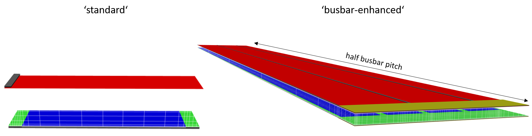
Notably one can set a different contact pitch at the front and rear side, which must otherwise be closely related in common unit-cell simulation, usually being restricted to equal, half or double. Quokka3 finds the least-common multiplier of the two pitches, and this way creates the “true” symmetry element for any pitch combination. However, the user should take care to use sensible numbers, to prevent a very large mesh and simulation time. But there is no limit on practically realizable pitch combinations in Quokka3, as at the far end one can define a full cell with the actual geometry (using the generic syntax).
Conduction types and polarities (n-type or p-type) of all features are ignored, but defined globally via ‘FrontMetalPolarity’ and ‘RearMetalPolarity’, which must be opposite.
| parameter | (recommended) value range | description or reference to ‘generic’ syntax |
|---|---|---|
| Solver | same as for ‘generic’ Syntax | |
| Optical | same as for ‘generic’ Syntax | |
| Material | same as for ‘generic’ Syntax | |
| Bulk | same as for ‘generic’ Syntax | |
| ExternalCircuit | same as for ‘generic’ Syntax | |
| Sweep | same as for ‘generic’ Syntax | |
| UnitCellType | ‘standard’, ‘busbar-enhanced’ | which type of unit cell to simulate; ‘busbar-enhanced’ covers half of a busbar width and half of a finger length |
| CellThickness | 0.1..200 \(\mu m\) | cell thickness excluding metallization |
| FullFrontSkin | full-area front skin, same as SkinFeature group excluding Geometry group | |
| LocalFrontSkin.Enable | 1 / 0* | whether to define an additional localized skin at the front, aligned to the front contact geometry |
| LocalFrontSkin.Width | 1..200 \(\mu m\) | width of localized front skin, defaults to ‘FrontContactWidth’ if not given |
| LocalFrontSkin | local front skin, same as SkinFeature group excluding Geometry group | |
| LocalFrontBusbarSkin.Enable | 1 / 0* | whether to define an additional skin at the front, aligned to the front busbar geometry |
| LocalFrontBusbarSkin | local front busbar skin, same as SkinFeature group excluding Geometry group | |
| LocalFrontContactSkin.Enable | 1 / 0* | whether to define an additional skin at the front, aligned to the front contact geometry |
| LocalFrontContactSkin | local front contact skin, same as SkinFeature group excluding Geometry group | |
| FrontContactShape | ‘full’, ‘line’, ‘dot’, ‘dash’ | contact shape of front side; ‘dot’ is approximated by a square |
| FrontContactWidth | 1..200 \(\mu m\) | width of front contacts |
| FrontContactPitch | 100..5000 \(\mu m\) | main pitch of front contacts and fingers |
| FrontContactLength | 10..1000 \(\mu m\) | length of ‘dash’ contacts |
| FrontContactSpacing | 10..1000 \(\mu m\) | spacing / secondary pitch of front contacts, for ‘dot’ and ‘dash’ |
| FrontContact | same as ContactFeature group excluding Geometry group | |
| FrontMetalShape | ‘full’, ‘H-pattern’ | shape of the front metallization; ‘H-pattern’ includes a busbar for the ‘busbar-enhanced’ unit cell type |
| FrontMetalPolarity | ‘n-type’, ‘p-type’ | polarity of front side |
| FrontMetalRsheet | 1e-3..1 \(\Omega\) | sheet resistance of the front metallization, only applicable if the metal is solved by finite differences |
| FrontFingerWidth | 1..200 \(\mu m\) | width of front fingers |
| FrontFingerShadingFraction | 0..1 | shading fraction of the front fingers to account for reflected and scattered light still contributing to generation |
| FullRearSkin | same as SkinFeature group excluding Geometry group | |
| LocalRearSkin.Enable | 1 / 0* | whether to define an additional skin at the rear, aligned to the rear contact geometry |
| LocalRearSkin.Width | 1..200 \(\mu m\) | width of localized rear skin, defaults to ‘RearContactWidth’ if not given |
| LocalRearSkin | local rear skin, same as SkinFeature group excluding Geometry group | |
| LocalRearBusbarSkin.Enable | 1 / 0* | whether to define an additional skin at the rear, aligned to the rear busbar geometry |
| LocalRearBusbarSkin | local rear busbar skin, same as SkinFeature group excluding Geometry group | |
| LocalRearContactSkin.Enable | 1 / 0* | whether to define an additional skin at the rear, aligned to the front contact geometry |
| LocalRearContactSkin | local rear contact skin, same as SkinFeature group excluding Geometry group | |
| RearContactShape | ‘full’, ‘line’, ‘dot’, ‘dash’ | contact shape of rear side; ‘dot’ is approximated by a square |
| RearContactWidth | 1..200 \(\mu m\) | width of rear contacts |
| RearContactPitch | 100..5000 \(\mu m\) | main pitch of rear contacts and fingers; can be different to front contact pitch, but a reasonably low least-common-multiplier should be ensured |
| RearContactLength | 10..1000 \(\mu m\) | length of ‘dash’ contacts |
| RearContactSpacing | 10..1000 \(\mu m\) | spacing / secondary pitch of rear contacts, for ‘dot’ and ‘dash’ |
| RearContact | same as ContactFeature group excluding Geometry group | |
| RearMetalShape | ‘full’, ‘H-pattern’ | shape of the front metallization; ‘H-pattern’ includes a busbar for the ‘busbar-enhanced’ unit cell type |
| RearMetalPolarity | ‘n-type’, ‘p-type’ | polarity of rear side, must be opposite to front side |
| RearMetalRsheet | 1e-3..1 \(\Omega\) | sheet resistance of the rear metallization, only applicable if the metal is solved by finite differences |
| RearFingerWidth | 1..200 \(\mu m\) | width of rear fingers |
| RearFingerShadingFraction | 0..1 | shading fraction of the rear fingers to account for reflected and scattered light still contributing to generation |
| BusbarPitch | 10e3..100e3 \(\mu m\) | busbar pitch |
| FrontBusbarWidth | 100..2000 \(\mu m\) | front busbar width |
| FrontBusbarContactEnable | 1 / 0 | whether to model contacted or non-contacted busbars |
| FrontBusbarShadingFraction | 0..1 | shading fraction of the front busbars to account for reflected and scattered light still contributing to generation |
| RearBusbarWidth | 100..2000 \(\mu m\) | rear busbar width |
| RearBusbarContactEnable | 1 / 0 | whether to model contacted or non-contacted rear busbars |
| RearBusbarShadingFraction | 0..1 | shading fraction of the rear busbars to account for reflected and scattered light still contributing to generation |
front and rear contact full cell
This syntax is similar to the ‘front and rear contact unit cell’ in that it defines a both-sides contacted solar cell with H-patterned or full-area metallization at the front and rear. It differs in that it defines the geometry based on a full-cell view, meaning cell size, busbar and finger numbers, instead of the respective pitches. Most notably, it accounts for edge effects, featuring the optional inclusion of a redundant-line. It further supports a shingle cell layout.
The syntax allows different solution domains to represent the full cell by the ‘FullCellDomainType’ parameter:
- ‘full’ builds the 3D geometry of the entire cell
- ‘half-symmetry’ and ‘quarter-symmetry’ builds the respective symmetry element only
- ‘multi-domain’, see below
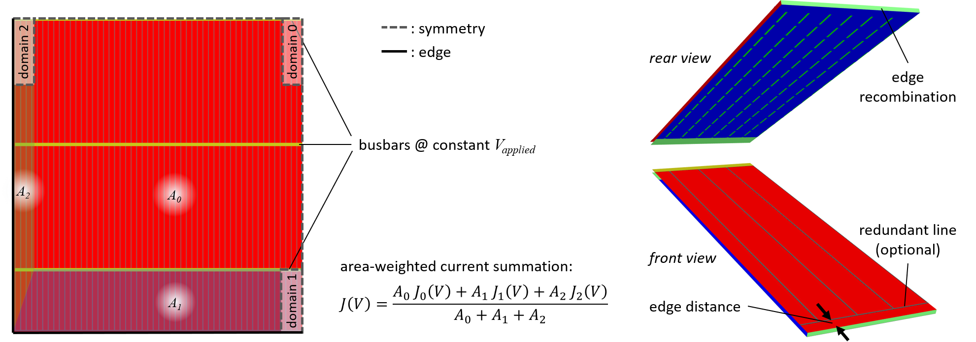
multi-domain approach
The multi-domain approach automatically constructs multiple different solution domains comprising an inner domain and one or two edge domains (for a shingle layout there is only one edge domain). By the sole assumption that the busbars have a constant potential, which is inherit to this simplified syntax anyway, the full-cell characteristics including edge effects can be accurately simulated with a fraction of the computational demand. This in particular enables to accurately simulate full-cell characteristics of more complex cell designs, e.g. featuring dot / dashed rear-contacts, as those would result in prohibitively large meshes for the other full-cell domain types.
An additional benefit is that by comparing the final result from the inner and edge domains the edge losses of the full cell design are directly quantified, whereas the other domain types would require an additional simulation (e.g. a busbar-enhanced unit-cell simulation) as an edge-loss-free reference point.
| parameter | (recommended) value range | description or reference to ‘generic’ syntax |
|---|---|---|
| Solver | same as for ‘generic’ Syntax | |
| Optical | same as for ‘generic’ Syntax | |
| Material | same as for ‘generic’ Syntax | |
| Bulk | same as for ‘generic’ Syntax | |
| ExternalCircuit | same as for ‘generic’ Syntax | |
| Sweep | same as for ‘generic’ Syntax | |
| FullCellDomainType | ‘full’, ‘half-symmetry’, ‘quarter-symmetry’, ‘multi-domain’ | which type of solution domain(s) to construct |
| CellThickness | 0.1..200 \(\mu m\) | cell thickness excluding metallization |
| CellSizeX | 1e4..5e5 \(\mu m\) | full cell size in X-dimension |
| CellSizeY | 1e4..5e5 \(\mu m\) | full cell size in Y-dimension |
| RedundantLineEnable | 1 / 0 | Whether to include a redundant-line |
| CellOverlap | 0..5000 \(\mu m\) | overlap of shingled cells |
| EdgeDistanceBusbar | 0..5000 \(\mu m\) | distance between the edge of the busbar and the edge of the cell (applicable to shingle cell only) |
| FrontEdgeDistanceX | 0..1000 \(\mu m\) | distance between metal and edge in X-direction |
| FrontEdgeDistanceY | 0..1000 \(\mu m\) | distance between metal and edge in Y-direction |
| RearEdgeDistanceX | 0..1000 \(\mu m\) | distance between metal and edge in X-direction |
| RearEdgeDistanceY | 0..1000 \(\mu m\) | distance between metal and edge in Y-direction |
| BusbarNumber | 1..50 | numnber of busbars (not applicable for shingle cell) |
| FrontBusbarWidth | 100..2000 \(\mu m\) | front busbar width |
| FrontBusbarContactEnable | 1 / 0 | whether to model contacted or non-contacted busbars |
| FrontBusbarShadingFraction | 0..1 | shading fraction of the front busbars to account for reflected and scattered light still contributing to generation |
| RearBusbarWidth | 100..2000 \(\mu m\) | rear busbar width |
| RearBusbarContactEnable | 1 / 0 | whether to model contacted or non-contacted rear busbars |
| RearBusbarShadingFraction | 0..1 | shading fraction of the rear busbars to account for reflected and scattered light still contributing to generation |
| FullFrontSkin | full-area front skin, same as SkinFeature group excluding Geometry group | |
| LocalFrontSkin.Enable | 1 / 0* | whether to define an additional localized skin at the front, aligned to the front contact geometry |
| LocalFrontSkin.Width | 1..200 \(\mu m\) | width of localized front skin, defaults to ‘FrontContactWidth’ if not given |
| LocalFrontSkin | local front skin, same as SkinFeature group excluding Geometry group | |
| LocalFrontBusbarSkin.Enable | 1 / 0* | whether to define an additional skin at the front, aligned to the front busbar geometry |
| LocalFrontBusbarSkin | local front busbar skin, same as SkinFeature group excluding Geometry group | |
| LocalFrontContactSkin.Enable | 1 / 0* | whether to define an additional skin at the front, aligned to the front contact geometry |
| LocalFrontContactSkin | local front contact skin, same as SkinFeature group excluding Geometry group | |
| FrontContactShape | ‘full’, ‘line’, ‘dot’, ‘dash’ | contact shape of front side; ‘dot’ is approximated by a square |
| FrontContactWidth | 1..200 \(\mu m\) | width of front contacts |
| FrontContactNumber | 1..1000 | number of front contact lines (fingers) |
| FrontContactLength | 10..1000 \(\mu m\) | length of ‘dash’ contacts |
| FrontContactSpacing | 10..1000 \(\mu m\) | spacing / secondary pitch of front contacts, for ‘dot’ and ‘dash’ |
| FrontContact | same as ContactFeature group excluding Geometry group | |
| FrontMetalShape | ‘full’, ‘H-pattern’, ‘shingle’ | shape of the front metallization |
| FrontMetalPolarity | ‘n-type’, ‘p-type’ | polarity of front side |
| FrontMetalRsheet | 1e-3..1 \(\Omega\) | sheet resistance of the front metallization, only applicable if the metal is solved by finite differences |
| FrontFingerWidth | 1..200 \(\mu m\) | width of front fingers |
| FrontFingerShadingFraction | 0..1 | shading fraction of the front fingers to account for reflected and scattered light still contributing to generation |
| FullRearSkin | same as SkinFeature group excluding Geometry group | |
| LocalRearSkin.Enable | 1 / 0* | whether to define an additional skin at the rear, aligned to the rear contact geometry |
| LocalRearSkin.Width | 1..200 \(\mu m\) | width of localized rear skin, defaults to ‘RearContactWidth’ if not given |
| LocalRearSkin | local rear skin, same as SkinFeature group excluding Geometry group | |
| LocalRearBusbarSkin.Enable | 1 / 0* | whether to define an additional skin at the rear, aligned to the rear busbar geometry |
| LocalRearBusbarSkin | local rear busbar skin, same as SkinFeature group excluding Geometry group | |
| LocalRearContactSkin.Enable | 1 / 0* | whether to define an additional skin at the rear, aligned to the front contact geometry |
| LocalRearContactSkin | local rear contact skin, same as SkinFeature group excluding Geometry group | |
| RearContactShape | ‘full’, ‘line’, ‘dot’, ‘dash’ | contact shape of rear side; ‘dot’ is approximated by a square |
| RearContactWidth | 1..200 \(\mu m\) | width of rear contacts |
| RearContactNumber | 1..1000 | number of rear contact lines (fingers); for the multi-domain approach a reasonable large least-common-multiplier with FrontContactNumber is desirable to not result in large mesh sizes |
| RearContactLength | 10..1000 \(\mu m\) | length of ‘dash’ contacts |
| RearContactSpacing | 10..1000 \(\mu m\) | spacing / secondary pitch of rear contacts, for ‘dot’ and ‘dash’ |
| RearContact | same as ContactFeature group excluding Geometry group | |
| RearMetalShape | ‘full’, ‘H-pattern’, ‘shingle’ | shape of the front metallization |
| RearMetalPolarity | ‘n-type’, ‘p-type’ | polarity of rear side, must be opposite to front side |
| RearMetalRsheet | 1e-3..1 \(\Omega\) | sheet resistance of the rear metallization, only applicable if the metal is solved by finite differences |
| RearFingerWidth | 1..200 \(\mu m\) | width of rear fingers |
| RearFingerShadingFraction | 0..1 | shading fraction of the rear fingers to account for reflected and scattered light still contributing to generation |
1D detailed homojunction cell
The ‘1D detailed homojunction cell’ syntax defines 1D semiconductor device consisting of a homogenous material, i.e. having skins of ‘near-surface’ type at the front and the rear.
| parameter | (recommended) value range | description or reference to ‘generic’ syntax |
|---|---|---|
| CellThickness | 0.1..200 \(\mu m\) | cell thickness excluding metallization |
| Solver | same as for ‘generic’ Syntax | |
| Material | same as ‘generic’ Syntax | |
| Optical | same as ‘generic’ Syntax | |
| Bulk.Electrical | same as ‘generic’ Syntax | |
| Bulk.Material | same as ‘generic’ Syntax | |
| Mesh | same as Bulk.Mesh group; at least ‘standard’ quality is recommended, ‘user’ is not supported | |
| ExternalCircuit | same as for ‘generic’ Syntax | |
| Sweep | same as for ‘generic’ Syntax |
The near-surface skins, contacts and metal at the front and rear are defined via the Front and Rear groups:
Front / Rear settings groups:
| parameter | (recommended) value range | description or reference to ‘generic’ syntax |
|---|---|---|
| .Mesh | same as for detailed skin settings; optional parameter | |
| .Lumped.Optical | same as for skin feature settings | |
| .DopingProfile | same as for detailed skin settings | |
| .ActiveProfile | same as for detailed skin settings | |
| .Surface | same as for detailed skin settings | |
| .Contact | same as for ContactFeature | |
| .MetalPolarity | ‘n-type’, ‘p-type’ | polarity of the potential applied to the respective side; front and rear must be opposite |
| .MetalWorkFunction | 0..10 \(eV\) | only used for a Schottky-type contact where the barrier height is derived from the workfunctions |
near-surface skin
With the ‘near-surface skin’ syntax one can define a ‘semiconductor skin’ domain which represents a near-surface region. It is useful for example to simulate the (injection dependent) \(J_{0,skin}\) of a highly doped or passivated silicon surface.
| parameter | (recommended) value range | description or reference to ‘generic’ syntax |
|---|---|---|
| Solver.SolutionType | ‘skin single-point’, ‘skin QE-curve’ | solution types applicable to the skin solver |
| Solver.Skin.QFPsplit | 0..2 \(V\) | bulk-side quasi-Fermi potential split; defines maximum value for \(\phi_{split}\) variation |
| Solver.Skin.Jterm | -200..200 \(mA/cm^2\) | net current density through skin; defines maximum absolute value for \(J_{term}\) variation |
| Solver.Skin.Resolution | 1..100 | how many data points to use for \(\phi_{split}\) (and \(J_{term}\)) variation |
| Material | same as ‘generic’ Syntax | |
| Optical | same as ‘generic’ Syntax, except: no ‘uniform-Jgen’ for defined generation; no rear illumination; no Z definition for Text-Z model; no Luminescence | |
| DepthType | ‘auto’, ‘user’ | how to determine the depth of the near-surface region |
| DepthUser | 0..10 \(µm\) | user-defined depth of near-surface region (make sure it extends to the quasi-neutral bulk) |
| Mesh | same as for detailed skin settings | |
| BackgroundDoping | same as for bulk background doping group | |
| DopingProfile | same as for detailed skin settings | |
| ActiveProfile | same as for detailed skin settings | |
| Recombination | same as bulk recombination group | |
| Surface | same as for detailed skin settings | |
| Contact.Enable | 1 / 0 | whether skin is contacted or not |
| Contact | same as ContactFeature.Electrical | |
| MetalPolarity | ‘n-type’, ‘p-type’ | polarity of the potential applied to the skin’s contact |
| MetalWorkFunction | 0..10 \(eV\) | workfunction of metal; only used if contact barrier height is set to ‘from workfunction’ |
| Sweep | same as for ‘generic’ Syntax |
Quokka 2.2.5 FRC
This syntax provides backwards compatibility to Quokka2. It can read a Quokka2 settingsfile by adding the “Syntax=‘Quokka 2.2.5 FRC’” line, provided the following:
- Quokka3 supports only the ‘FRC’ (front- and rear-contact) version of Quokka2, not the ‘IBC’ one
- No Matlab-like scripting functionality is supported: the settingsfile must not contain any variables or expressions (e.g. “50/2” as a scalar value is NOT supported)
- Due to the above, no analytical expression for surface recombination is supported
- Optimizer settings are disregarded
- Import of .xls files is not supported
- The sweep syntax is not supported, but can be changed manually into the Quokka3 sweep syntax using the Quokka2 parameter names
- Settings for material properties are ignored (Quokka3 defaults for Si are applied)
While results should be very similar between Quokka2 and Quokka3, some minor differences due to differences in material models cam be expected.
Output
Simulation results are output in two different files:
- A HDF5 (.h5) file, containing all rendered results. HDF5 is an open-source file format specifically developed to store large datasets of different types into a group-structure. Data can be browsed, read and further processed by many scientific software tools (e.g. Matlab, Mathematica, Python, …). It also contains metadata, e.g. sweep parameter names, units, used version, etc.
- A XML (.xls) spreadsheet file, containing a subset of the results and can be conveniently opened in Excel. You can safely ignore the header-warning issued by Excel when opening the file.
What kind of results are rendered by Quokka3 is dependent on the simulation setup, in particular the solution type (and whether it contains a unique operating point), and the sweep settings. There are 4 different types of results: Scalar, Curves, Maps and Spatial results. They are stored in Groups with the respective name in the HDF5 file, and in separate sheets for the XML file.
- Scalar: a single numeric value (e.g. Voc). If a sweep is defined, this will be an array of values according to the sweep dimensions. For a two-dimensional sweep (i.e. using GroupA and GroupB sweep parameters), Scalars are stored as 2D arrays in the hdf5 file, which easily allows for e.g. contour plots. In the XML file the results from a 2D sweep are linearized.
- Curves: curves are rendered only for ‘curve’-solution types. For a sweep, the set of curves for each sweep point is stored in a separate subgroup named ‘/Sweep(ia,ib)/’ in the HDF5 file.
- Maps: currently luminescence maps and a power loss map are rendered. They are 2D arrays in the XY plane, and are only stored in the HDF5 file. The hyperspectral luminescence map has one more dimension for the wavelength. For a sweep, equivalent subgroups as for Curves are created. Maps may not be stored by default, but can be forced to be stored.
- Spatial: In the HDF5 file spatial data is always stored as 3D arrays, regardless of the dimensions of the solution domain. Note that the order of the dimensions is Z, X, Y. It also contains vectors for the element center and face positions in each coordinate direction. Some spatial results, e.g. current densities, are defined at element face positions rather than centers, and have consequently one more data point in the respective coordinate direction. In the XML file only 1D spatial data is stored. For a sweep, equivalent subgroups as for Curves are created. Spatial data may not be stored by default, but can be forced to be stored.
#References
Brendel, R., M. Hirsch, R. Plieninger, and J. J. H. Werner. 1996. “Quantum Efficiency Analysis of Thin-Layer Silicon Solar Cells with Back Surface Fields and Optical Confinement.” IEEE Transactions on Electron Devices 43 (7): 1104–13.
Fell, Andreas, Keith R. McIntosh, and Kean C. Fong. 2016. “Simplified Device Simulation of Silicon Solar Cells Using a Lumped Parameter Optical Model.” IEEE Journal of Photovoltaics, 1–6. https://doi.org/10.1109/JPHOTOV.2016.2528407.
Fell, A., J. Schön, M. Müller, N. Wöhrle, M. C. Schubert, and S. W. Glunz. 2018. “Modeling Edge Recombination in Silicon Solar Cells.” IEEE Journal of Photovoltaics PP (99): 1–7. https://doi.org/10.1109/JPHOTOV.2017.2787020.
Green, Martin A. 2002. “Lambertian Light Trapping in Textured Solar Cells and Light–Emitting Diodes: Analytical Solutions.” Progress in Photovoltaics: Research and Applications 10 (4): 235–41.