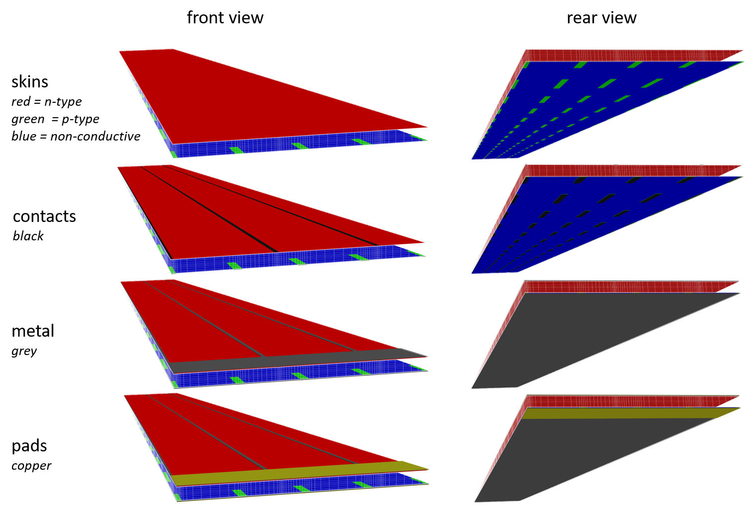
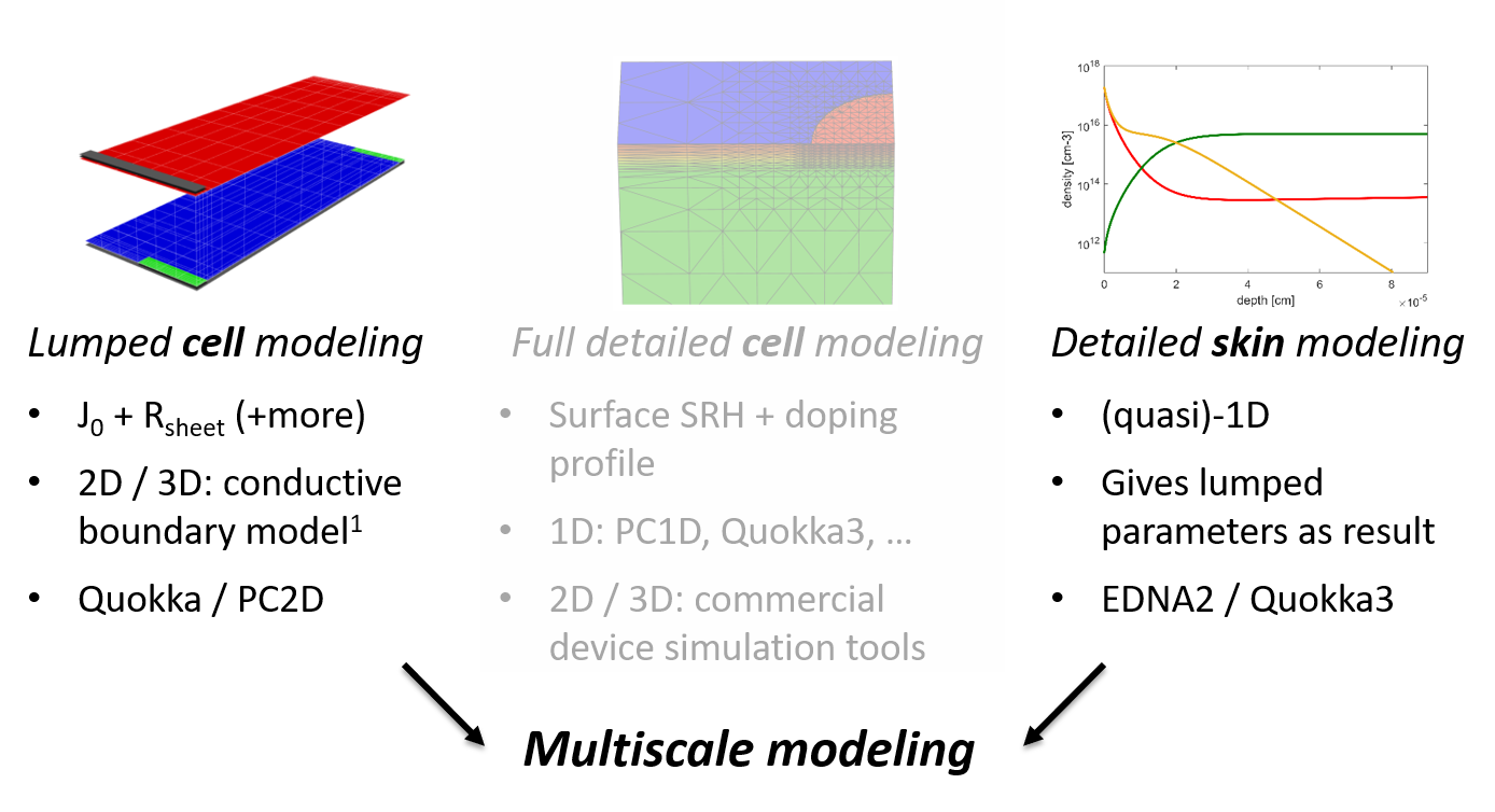
Concept: Bulk, Skin, Contact, Metal and Pad
In Quokka3 a solar cell is conceptualized into separate regions:
- The bulk: it is the main absorber, and (for Si solar cells) can well be assumed to be everywhere quasi-neutral if defined to exclude the near-surface regions. Only the bulk is discretized in the depth coordinate.
- The skin layer: skins are region-wise homogenous areas which cover everything between the quasi-neutral bulk and either the actual surface or the contact to the metal. Typical skins are contacted or non-contacted diffused surfaces, or passivated surfaces (including the inversion or accumulation layer). Quokka3 supports skins to be defined by lumped inputs (lumped skin) e.g. sheet resistance and \(J_0\), or detailed inputs (detailed skin) e.g. doping profile and surface SRH.
- The contact layer: contacts in Quokka3 define the interface where current can flow between the skin and the metal. Where no contact is defined between the skin and the metal layer, they are assumed to be perfectly isolated.
- The metal layer: represents finger and busbar geometry and accounts for lateral current flow within them (if it is set to be modelled by ‘finite-differences’)
- The pad layer: pads represent the probes or solder pads to which the plus and minus pole is applied, and through which the current is extracted. They are important only when solving current transport in the metal layer, because otherwise the entire metal geometry effectively represents a probe applying a ‘constant potential’.
The key of Quokka3 to make it numerically efficient and specifically useful for wafer-based silicon solar cells, is to numerically treat the skins always as a parameterized boundary condition when solving carrier transport in the bulk. The main lumped parameters to describe a skin as a boundary condition are its recombination property \(J_{0,skin}\), and its sheet resistance \(R_{sheet}\), which are well-established to sufficiently describe of a Si solar cell in many cases. Quokka3 notably can also model skins in detail and then use a more general parameterization, which is applied in the multiscale modeling, ensuring high accuracy also for arbitrary skin properties.
Meshing
Quokka3 uses a structured, orthogonal and non-equidistant mesh to discretize the solution domain and build the finite differences expressions. This means that the solution domain is always strictly cuboidal, and that the geometry definition of the device needs to consist of primitive rectangular geometric features aligned to the coordinate axes. The geometric features are arbitrary in number, position and size, resulting in a generic geometry definition within this rectangular restriction. As an exemption from this a circle as a primitive shape is also supported. It is however recommended in most cases to instead use a square shape with equal area, which requires a much smaller mesh for accurate discretization. The orthogonal mesh is well suited for silicon solar cells, as most cases of interest can be approximated by rectangular device geometries.
This type of mesh comes with the benefits of a rapid and fully automated meshing algorithm (seconds for millions of elements) requiring minimal attention from the user, and of fast and robust electrical solver numerics based on finite differences.
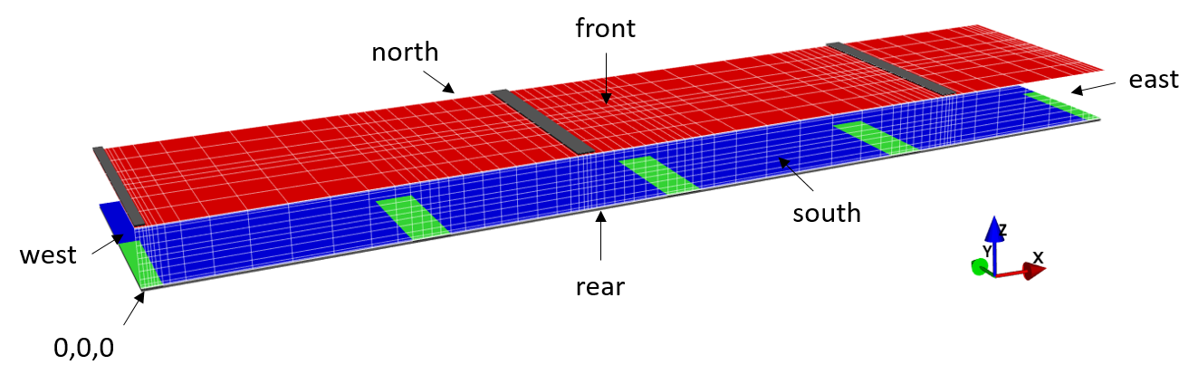
The 3D solution domain of Quokka3 for above mentioned reasons is strictly cuboidal. To distinguish the boundary planes they are named ‘front’, ‘rear’, ‘east’, ‘west’, ‘north’ and ‘south’ side. For a 2D simulation, the y-coordinate and consequently the ‘north’ and ‘south’ sides are disregarded. For a 1D simulation also the x-coordinate is disregarded. The origin of the coordinate system is defined at the ‘rear’-‘west’-‘south’ corner, which notably means that \(z=0\) corresponds to the rear side, and not to the front surface as in many other tools.
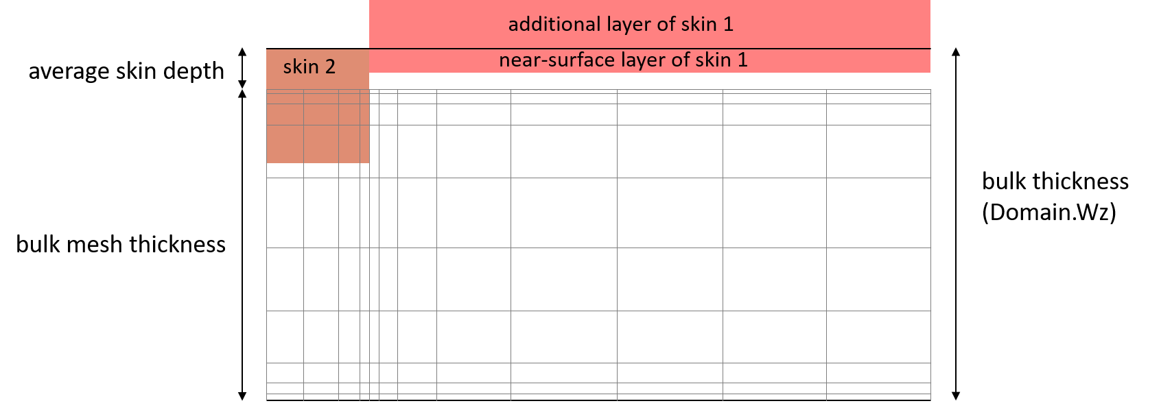
The bulk mesh covers only the bulk excluding the skin depth, which precisely is the skin’s near-surface layer thickness only. A problem arises if on one side skins with different depths are defined, as the bulk mesh can only have a unique size in z-coordinate. In such a case, Quokka3 calculates the area-average of the skin-depths, and subtracts this average from the user-defined bulk thickness. As far as possible Quokka3 ensures consistency, e.g. still using the correct individual skin depth for optical and detailed electrical modeling. However, for bulk carrier transport, only the single average skin depth can be assumed. This is a good assumption if the differences in skin depths are small compared to the device thickness, but may lead to some inaccuracy otherwise.
Optical modeling
Optical modeling in Quokka3 can be separated into two cases: modeling optics for determining the generation rate in the device, and modelling luminescence to determine the emitted luminescence spectrum and intensity. If both are iteratively coupled, the effect of photon-recycling can be modelled (NOT YET IMPLEMENTED).
Solving generation: the Text-Z model
Besides directly setting the generation via user-defined generation profile, Quokka3 supports spectrally resolved optical modeling by the Text-Z model. It’s a further simplification of the Basore-model (Rand and Basore 1991; Basore 1993), requiring only the (spectrally dependent) input parameters external front surface transmission \(T_{ext}\) and pathlength enhancement factor \(Z\). It is described in detail in (Fell, McIntosh, and Fong 2016).
The main features of the Text-Z model are:
- Being (semi-) analytical, it is rapid for all purposes
- The determined generation profiles are accurate for non-extreme wafer-based silicon solar cells
- The input parameters can be derived either from experiments or detailed optical simulations (e.g. ray tracing + transfer matrix), providing the most suitable interface to detailed optical modelling tools
- Being spectrally resolved, it enables rapid optical modeling for quantum efficiency (QE) simulations
- It is compatible with the skin concept, i.e. accounts for generation and collection efficiency in the skin
- The input parameters are, to good approximation, independent of temperature and the wafer thickness (the latter if additionally a parameterization of \(Z\) is used (McIntosh and Baker-Finch 2015)), meaning that those quantities can be varied within Quokka3 without re-doing detailed optical modeling or characterization.
Definition of optical parameters
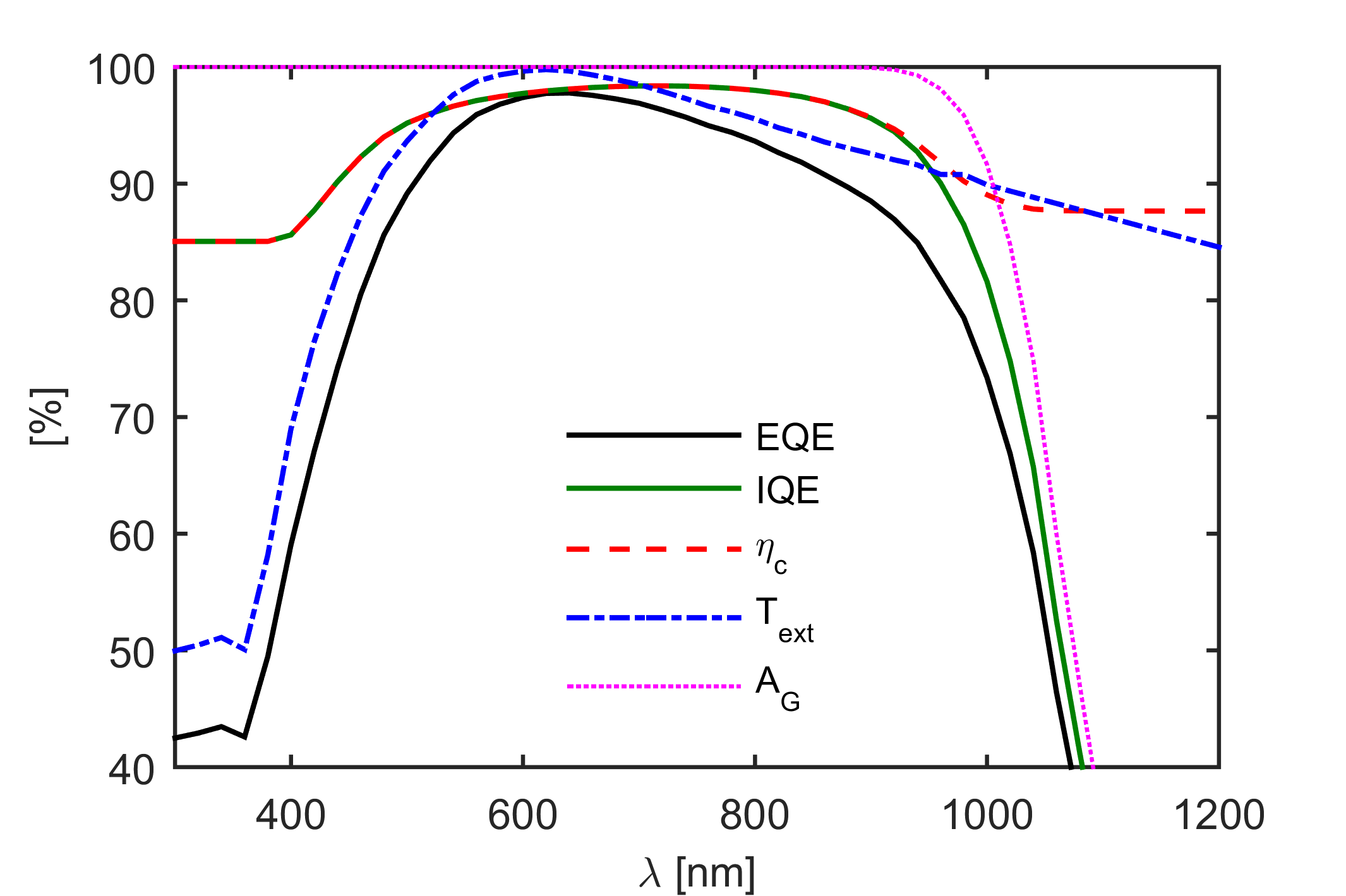
Above the spectral optical parameters important in the context of the Text-Z model are shown. They all influence the measurable external quantum efficiency (EQE) of the device. The input parameter \(Z\) is directly related to the absorbed fraction of transmitted photons, \(A_G\), and the internal quantum efficiency (IQE). \[ EQE(\lambda)=T_{ext}(\lambda)IQE(\lambda) \]
\[ IQE(\lambda)=A_G(\lambda)\eta_c(\lambda) \]
\[ A_G(\lambda)=1-\exp\left(-\alpha(\lambda)Z(\lambda)W\right) \]
Notably, for a given spectrum and device thickness \(W\), the device’s generation current \(J_G\) is directly defined by the Text-Z model’s input parameters. Consequently, this most important quantity is ensured to be consistent, e.g. when the inputs are derived from ray tracing software. \[ J_G=q\int_{0}^{\infty}{I(\lambda)T_{ext}(\lambda)\left(1-\exp\left(-\alpha(\lambda)Z(\lambda)W\right)\right)d\lambda} \]
Calculating the generation profile
The Text-Z model is based on the faceted surface model [ref Basore]. It accounts for different effective path angles in the near-surface region (i.e. in the skin) and in the bulk. This way, both the short-wavelength and long-wavelength IQE is correctly modelled. Differently to the Basore model, light reflected at the rear-surface is not followed further by internal optical properties of the surfaces. Rather, the remaining generation after the first path \(l_1\) is distributed equally over the device thickness: \[ G(\zeta,\lambda)=G_1(\zeta,\lambda)+W^{-1}I(\lambda)T_{ext}(\lambda)\left(\exp\left(-\alpha(\lambda)l_1\right)-\exp\left(-\alpha(\lambda)Z(\lambda)W\right)\right) \]
Different ways to define Z
Quokka3 supports various options to define Z:
- Directly user-defined, i.e. the user provides Z values as a function of wavelength, or better as a function of absorption coefficient. Such Z values can be derived e.g. via a ray-tracing software, or via other optical modeling external to Quokka3.
- Choosing a limit for light-trapping
- \(4n^2\): well-known limit where \(Z(\lambda)=4(n(\lambda))^2\); notably it assumes zero absorption, and is thus valid for very weakly absorbing wavelengths only.
- (Green 2002): Green did improve over the \(4n^2\) limit by considering the effect of absorption, thus providing a more realistic upper limit of light trapping in a device: \(Z(\lambda) = 4 + \frac{\ln\left((n(\lambda))^2 + \left(1 - (n(\lambda))^2\right)\exp(-4\alpha (\lambda)W)\right)}{\alpha (\lambda)W}\)
- A parameterization of Z
- Calculating Z locally from the internal optical properties of the opposing skin’s. This is the only option capable of defining spatial variation in the light trapping properties of the device, as the other options use a global Z for the entire device.
Z parameterization
A parameterization to describe the dependence of \(Z\) on the wavelength, or more fundamentally on the absorption-coefficient, was derived in (McIntosh and Baker-Finch 2015): \[ Z(\alpha)=Z_\infty+\frac{1}{\alpha Z_pW}\ln\left(\frac{Z_0}{Z_\infty}-\left(\frac{Z_0}{Z_\infty}-1\right)\exp\left(-\alpha Z_\infty Z_pW\right)\right) \] The benefits arising from the \(Z\) parameterization are the following:
- Light trapping is accurately described by the 3 parameters \(Z_0\), \(Z_\infty\) and \(Z_p\) only, instead of requiring a full spectrally dependent curve.
- The parameters are specific to the optical properties of the surfaces only, i.e. independent of the device thickness \(W\). As also \(T_{ext}\) is independent of \(W\), this means that \(W\) can be varied in Quokka3 without adjusting optical inputs, yielding correct changes in generation.
- The parameters are, to good approximation, independent of temperature, allowing variation of temperature without adjusting optical inputs. See next section for details.
Local Z from skin properties
The model to calculate Z from the internal optical properties of two opposing skins is based on (Brendel et al. 1996). Note that in the following “front” means the illuminated side, and “rear” the non-illuminated side. The required lumped optical input parameters are:
- the facet angle of the front (i.e. illuminated) side texture
- the average (or nth-pass) internal reflectance of the skin \(R_{front,avg}\) and \(R_{rear,avg}\)
- for the front (i.e. illuminated) side optionally the specular reflectance \(R_{front,spec}\) (for the rear side, or if not given for the front side, it is assumed to be equal to the average reflectance)
- for the rear (i.e. non-illuminated) side the Lambertian fraction \(\Lambda_{rear}\)
Z is then calculated via:
\(A_G(\alpha)=1-\exp\left(-\frac{\alpha W}{\cos(\Theta_1)}\right)+T_1R_{rear,avg}\left(1-\exp\left(-\frac{\alpha W}{\cos(\Theta_2)}\right)\right)+\frac{T_1R_{rear,avg}T_2R_{front,1}(1+T_nR_{rear,avg})}{1-T_n^2R_{front,avg}R_{rear,avg}} \left(1-\exp\left(-\frac{\alpha W}{\cos(\Theta_n)}\right)\right)\)
\(Z(\alpha)=-\frac{\ln(1-A_G(\alpha))}{\alpha W}\)
The quantities \(\Theta_1 (=\Theta_{bulk})\), \(\Theta_2\), \(\Theta_n\), \(T_1\), \(T_2\), \(T_n\) and \(R_{front,1}\) are derived from the inputs as described in (Brendel et al. 1996).
Note that in (Brendel et al. 1996) typical values for a random-pyramid textured surface with a 105 \(nm\) \(SiO_2\) AR coating where given as \(R_{front,avg}=0.93\) and \(R_{front,spec}=0.62\). It is stated that those values approximately hold also for other AR coatings, and can thus be considered a general useful approximation for a random-pyramid textured surface. The only 2 remaining inputs to adjust the light trapping are then the (average) rear reflectance and rear Lambertian fraction.
Temperature (in-)dependence
In (Fell, McIntosh, and Fong 2016) it was shown that both \(T_{ext}\) and \(Z\) can be approximately assumed temperature independent for typical silicon solar cell operating conditions. When using Quokka3’s Text-Z model it is therefore conveniently possible to vary the temperature without having to adjust any optical inputs, and get a correct prediction of the change in generation current.
This is due to the fact that temperature dependence of the optical properties is largely dominated by changes in the absorption coefficient \(\alpha(\lambda)\), which is a different function of wavelength for different temperatures. As mentioned in the Z parameterization, \(Z\) fundamentally is a function of \(\alpha\), which is the only wavelength- and temperature-dependent quantity. Therefore, \(Z\) is recommended to be defined as a function of \(\alpha\), or by its parameterization, and can then be considered independent of temperature. The reasoning is similar for the long-wavelength region of \(T_{ext}\). For the short-wavelength region of \(T_{ext}\) however, the wavelength-dependence can be considered temperature independent instead. Often for typical silicon solar cells the entire \(T_{ext}(\lambda)\) curve can well be considered temperature-independent.
Solving luminescence and photon-recycling
photon recycling not yet implemented
Electrical modeling
General semiconductor model equations
Current transport in a semiconductor is well established to be modelled by coupling the continuity equations for charge carrier transport with the Poisson equation, also known as the drift-diffusion model. In Quokka3, up to 4 charge carriers are considered in the 1D detailed solver, that is anions and cations additionally to electrons and holes. The following equations are given in the most general form to cover all effects considered in Quokka3. Note however that those equations are never solved in such generality, meaning a fully coupled transient solution of continuity and Poisson equations in 3D, including ion transport. Refer to the individual solver section to see under what specific assumptions those equations are solved.
Volume carrier transport
Electron and hole carrier transport is described by the respective continuity equation: \[ \frac{dn}{dt}=q(G-R_{el})-\nabla\vec{J}_{el} \]
\[ \frac{dp}{dt}=q(G-R_{hol})+\nabla\vec{J}_{hol} \]
Quokka uses the electrochemical or quasi-Fermi potentials \(\phi_{el}\) and \(\phi_{hol}\) as solution variables, from which the current density is calculated as: \[ \vec{J}_{el/hol}=\kappa_{el/hol}\nabla\phi_{el/hol} \] The conductivities \(\kappa_{el}\) / \(\kappa_{hol}\) are calculated from the respective mobility \(\mu_{el}\) / \(\mu_{hol}\) and carrier density: \[ \kappa_{el} = q\,n\,\mu_{el}, \kappa_{hol}=q\,p\,\mu_{hol} \] Ion transport can be modeled equivalently, with anions and cations as charge carriers, however without generation and recombination: \[ \frac{dc_{an}}{dt}=-\nabla\vec{J}_{an} \]
\[ \frac{dc_{cat}}{dt}=\nabla\vec{J}_{cat} \]
\[ \vec{J}_{an/cat}=\kappa_{an/cat}\nabla\phi_{an/cat} \]
The Poisson equation relates the electric field \(\vec{E}\) to the net charge density: \[ \nabla\varepsilon_r\varepsilon_0\vec{E}=q(N_D-N_A+p-n+c_{cat}-c_{an}-n_t) \] The electric field is the negative gradient of the electrostatic potential \(\varphi_e\): \[ \vec{E}=-\nabla\varphi_e \]
Carrier statistics
Electrons and holes
Carrier statistics relate the semiconductor band-structure (i.e. energy levels) to the carrier densities. Generally valid is the use of Fermi-Dirac statistics: \[ n=N_c\,F_{1/2}\left(\frac{\phi_{el}-E_c/q}{V_t}\right) \]
\[ p=N_v\,F_{1/2}\left(-\frac{\phi_{hol}-E_v/q}{V_t}\right) \]
Here \(F_{1/2}()\) denotes the half-order Fermi integral. The conduction and valence band edges can be calculated from the band gap and the electrostatic potential: \[ E_c=-q\,\varphi_e+E_{g,0}/2-\delta E_{BGN,c} \]
\[ E_v=-q\,\varphi_e-E_{g,0}/2+\delta E_{BGN,v} \]
An important quantity is the intrinsic carrier density \(n_i\), which is related to the density of states and the band gap: \[ n_{i,0}^2=n_0p_0=N_cN_v\exp\left(-\frac{E_{g,0}}{q\,V_t}\right) \] If band gap narrowing (BGN) becomes significant, the effective intrinsic carrier density is defined by: \[ n_{i,eff}^2=n_{i,0}^2\exp\left(\frac{\delta E_{BGN,c}+\delta E_{BGN,v}}{q\,V_t}\right) \]
If carrier densities (i.e. doping densities) are below \(10^{19} cm^{-3}\), Fermi-Dirac statistics can be simplified to the mathematically easier Boltzmann statistics, where the Fermi integral is replaced by an exponential function (Altermatt 2011). A well known expression derived from Boltzmann statistics is that the product of the carrier densities (pn-product) is directly related to the Fermi level split: \[ pn=n_{i,eff}^2\exp{\left(\frac{\phi_{el}-\phi_{hol}}{V_t}\right)} \]
Ions
For ions, Quokka3 uses Boltzmann statistics: \[ c_{an}=N_{0,an}\,\exp\left(\frac{\phi_{an}+\varphi_e}{V_t}\right) \]
\[ c_{cat}=N_{0,cat}\,\exp\left(-\frac{\phi_{cat}+\varphi_e}{V_t}\right) \]
Generation and recombination
The generation rate of electron-hole pairs \(G\) is the result of optical modeling.
Recombination of electrons and holes happens via 3 different mechanisms:
- Radiative recombination, \(R_{rad}\)
- Auger recombination, \(R_{aug}\)
- Defect recombination via Shockley-Read-Hall (SRH) formalism, \(R_{SRH}\), as described in (Shockley and Read Jr 1952)
The first two are unavoidable contributions due to the intrinsic material properties, and are thus called intrinsic recombination, \(R_{intrinsic}=R_{rad}+R_{aug}\). They are assumed fast enough to be considered (quasi-)steady-state, and the recombination rates are equal for electrons and holes.
General SRH
This section describes the general SRH formalism described in (Shockley and Read Jr 1952). General SRH can currently be enabled for a single bulk defect within the 1D-detailed solver only. The default way to model SRH for all other cases is by its simplified form.
SRH recombination happens via defects having their energy level \(E_t\) placed within the band gap, called traps in the general formalism. In Quokka3, \(E_t\) is defined as the value relative to the middle of the band gap. The total defect / trap density \(N_t\) is differentiated from the density of occupied traps \(n_t\), and its fraction is defined as \(f_t=\frac{n_t}{N_t}\). The recombination rates for electrons and holes are their net rates of capture and emission, and can become negative if emission is larger: \[ R_{SRH,el}=\frac{\left(1-f_t\right)(n-n_0)-(n_0+n_1)\left(f_t-f_{t0}\right)}{\tau_{n0}} \]
\[ R_{SRH,hol}=\frac{f_t(p-p_0)+(p_0+p_1)\left(f_t-f_{t0}\right)}{\tau_{p0}} \]
The equilibrium occupied fraction is defined as: \[ f_{t0}=\frac{1}{1+\frac{n_1}{n_0}} \] \(n_1\) and \(p_1\) are the carrier concentrations for the case that the respective Fermi level coincides with the defect level: \[ n_1=n_{i,eff}\exp\left(\frac{E_t}{q\,V_t}\right) \]
\[ p_1=n_{i,eff}\exp\left(-\frac{E_t}{q\,V_t}\right) \]
The fundamental electron and hole lifetimes \(\tau_{n0}\) and \(\tau_{p0}\) can be calculated from the capture cross sections \(\sigma_n\) and \(\sigma_p\) as: \[ \tau_{n0/p0}=\frac{1}{v_{th}\sigma_{n/p}N_t} \] (Only) for the general formalism, the continuity equation for the trap density needs to be solved: \[ \frac{dn_t}{dt}=R_{SRH,el}-R_{SRH,hol} \]
Simplified SRH
Commonly in silicon solar cell modeling the simplified form of the general SRH formalism is used, which assumes (quasi-)steady-state and that the occupied trap density is small compared to the excess carrier density, i.e. \(\frac{n-n_0}{p-p_0}\simeq1\), see discussion in (Macdonald and Cuevas 2003). This means essentially that the effect of trapping is negligible. Then the electron and hole recombination rates are equal and become the well-know expression: \[ R_{SRH,el}=R_{SRH,hol}=R_{SRH}=\frac{p\,n-n_{i,eff}^2}{\tau_{n0}(p_1+p)+\tau_{p0}(n_1+n)} \]
Solving the bulk with lumped skins: qn-bulk solver
The qn-bulk solver solves 3D carrier transport in the bulk, as well as 2D current transport in up to two layers on each side: the skin layer and the metal layer. The following assumptions are made, which are specifically scoped to be valid for typical silicon solar cells:
- bulk semiconductor transport with lumped skins only: semiconductor carrier transport is only modelled in the bulk. Anything happening in the skins is “lumped away” into boundary conditions, including the lateral current transport. Note that the user can still provide detailed inputs for the skins, in which case multiscale modeling is used.
- quasi-neutrality: as space-charge regions are “outsourced” into the skins, the bulk region where semiconductor carrier transport is modelled can well be assumed to be quasi-neutral. This should NOT be confused with low-injection. It also does NOT set charge density within the Poisson equation to zero, i.e. still results in the correct non-zero electric field. Quasi-neutrality in the bulk holds very well for any typical silicon solar cell condition.
- Boltzmann statistics: as within the bulk both doping and excess carrier densities are well below the critical values, Boltzmann carrier statistics can be used without loss of accuracy.
- steady-state only
- simplified SRH only, no ion transport
Volume equations
The main benefit from the quasi-neutrality assumption is that the carrier densities can be calculated without knowledge of the electrostatic potential. This way, the continuity equations can be solved without solving the Poisson equation, which greatly reduces numerical challenges and thus increases speed and robustness. That means NOT that quasi-neutrality is assumed for the Poisson equation, which would render the electric field to zero. Rather the electric field causing the drift currents is implicitly solved by solving the continuity equations, which is accurate if the quasi-neutrality assumption holds. \[ \nabla\vec{J}_{el}=q(G-R) \]
\[ \nabla\vec{J}_{hol}=-q(G-R) \]
Applying quasi-neutrality and Boltzmann statistics, the carrier densities can be calculated as: \[ n-n_0=p-p_0=\sqrt{\frac{(n_o+p_0)^2}{4}-\left(p_0n_0-n_{i,eff}^2\exp{\frac{\phi_{el}-\phi_{hol}}{V_t}}\right)}-\frac{n_0+p_0}{2} \] The electric field can be post-calculated once the solution for the Fermi levels has been found, either by the electron or hole density: \[ \varphi_e=-\left(\phi_{el}-V_t\ln{\left(\frac{n}{n_{i,eff}}\right)}\right)=-\left(\phi_{hol}+V_t\ln{\left(\frac{p}{n_{i,eff}}\right)}\right) \]
Boundary conditions
Symmetry / perfect edge boundary
By default, that is if no skin layer is defined on a specific side of the solution domain, a symmetry boundary condition is applied. Notably, the symmetry condition is equivalent to a perfect edge of the device, as it represents no current through and no recombination at this edge. \[ \vec{n}\vec{J}_{el/hol}=0 \]
Lumped skin and metal layer boundary
If skins are defined on a side of the solution domain, a single-element-deep mesh layer is added to the bulk’s mesh. Within that layer, lateral current transport is modelled by solving the continuity equation for the skin’s potential \(\varphi_{skin}\), where the conductivity is defined by the skin’s sheet resistance \(R_{sheet}\): \[ \nabla_t\left(\frac{1}{R_{sheet}}\nabla\varphi_{skin}\right)=\left(\vec{n}\vec{J}_{el}+\vec{n}\vec{J}_{hol}\right)-J_{cont} \] The right hand side is a source term, with \(\vec{n}\vec{J}_{el}+\vec{n}\vec{J}_{hol}\) being the net current density from the bulk into the skin, and \(J_{cont}\) the current density from the skin into the metal (i.e. through the contact).
Optionally on the front and rear side, an additional mesh layer can be added to solve current transport in the metal, which is called the ‘finite differences’ metal model type. The equation to solve is equivalent as for the skin layer, using the metal potential \(\varphi_{met}\), the metal sheet resistance, and \(J_{cont}-J_{pad}\) as the source term, where \(J_{pad}\) is the current from the metal into the pad.
The current density between the skin and metal layer, as well as between the metal and pad layer, is calculated via the respective contact resistivity: \[ J_{cont}=\frac{\varphi_{met}-\varphi_{skin}}{\rho_{cont}} \]
\[ J_{pad}=\frac{\varphi_{pad}-\varphi_{met}}{\rho_{pad}} \]
If current transport in the metal layer is modelled by ‘finite differences’, the pad potential \(\varphi_{pad}\) equals the applied voltage, which is defined to be zero for a ‘p-type’ polarity, and \(V_{int}\) for a ‘n-type’ polarity pad. If current transport in the metal is not modelled, the metal is assumed to be at ‘constant potential’, meaning that the metal potential is set to the applied voltage with the respective polarity, and the pads are consequently disregarded. The ‘constant potential’ metal model type should be the default choice when modeling common unit cells, as metal current transport within such a small domain size is usually not significant.
The current densities between the bulk and the skin form the actual boundary conditions for solving the bulk continuity equations. They, together with the lateral current transport, represent all physics happing within the skin in an effective way. As discussed in (Fell et al. 2017), for a steady-state solution, a single skin element can be considered a black-box electrical circuit element with a unique operating point defined by the potential differences between the skin and the neighboring elements. If the relation between the current densities \(\vec{n}\vec{J}_{el}\), \(\vec{n}\vec{J}_{hol}\) and \(J_{cont}\) and the potential differences is accurately known for all relevant operating points, the influence of the skin on the device characteristics is exactly described.
To parameterize the mentioned relation, an equivalent circuit model of a skin element is used. The parameterization can represent all possible steady-state current-potential relationships, and is thus generally valid for any properties of typical solar cell skins. The only relevant assumptions are taken for the case that lateral current transport in the skin is significant compared to lateral transport in the bulk: i) lateral current transport can be described via assuming a single skin potential, ii) it can be superimposed to vertical current transport, and iii) it is significant for one type of carrier only (named the majority carrier), i.e. the skin is either ‘p-type’ or ‘n-type’. Those assumptions hold well for most typical silicon solar cell skins, essentially because they are thin. The relevant potential differences reduce in this case to the bulk-side quasi-Fermi level split \(\phi_{split}=\phi_{el}-\phi_{hol}\), and the potential drop of majority carriers between the bulk and the skin layer \(\Delta\varphi_{maj}=\varphi_{skin}-\phi_{el/hol}\).
The parameters of the lumped skin model are the sheet resistance \(R_{sheet}\), the recombination property \(J_{0,skin}\), a generation current density \(J_{G,skin}\), the collection efficiency \(\eta_c\), and a vertical resistivity \(\rho_{skin}\). It also includes the contact to the metal via the contact resistivity \(\rho_{cont}\). The parameters have a good physical meaning in most cases. However they generally are mathematical parameters which, with full potential dependence, can represent any operating point of a typical skin. For example the vertical resistivity is commonly meaningful in representing e.g. space-charge-region resistance, but can become negative if the skin includes a top-cell of a tandem device.
When the vertical resistivity is negligible and the other parameters are assumed to be constant, the general skin parameterization is equivalent to the conductive boundary model, published in (Brendel 2012; Fell 2013) and used by Quokka2.
Quokka3 supports to define the lumped parameters directly as user inputs, with constant vertical resistance and sheet resistance, but allowing injection-dependence of the recombination, i.e. \(J_{0,skin}(\phi_{split})\). Alternatively, the skin solver can parameterize the results from a detailed solution of the skin and automatically apply it as the boundary condition to the qn-bulk solver, which is called multiscale modeling.
Ohmic mode
The qn-bulk solver also supports an ohmic mode, for which the following additional assumptions are taken:
- Solves a single potential only: any conductivity-type setting (‘n-type’ or ‘p-type’) is disregarded but assumed to be the same type for bulk and all skin features.
- No excitation: all conductivities and resistivities are constant values, meaning also the resulting device will be ohmic, i.e. having a constant resistance regardless of the applied voltage. No semiconductor physics other than a single continuity equation per element are solved.
- MIS contact exception: the only non-ohmic feature within the ohmic mode are MIS-type resistivities between the bulk and the skin, or between the skin and the metal. The boundary condition is described as the MIS_simple case of the [MIS contact][#miscontact] for the 1D detailed solver.
Solving detailed physics: 1D detailed solver
The 1D detailed solver can account for the full general models, however solving them in 1 dimension only. Meaning that the currents and the electric field have only a z-component, and \(\nabla\) is reduced to the derivation in z-direction. The 1D detailed solver can solve two types of solution domains:
- A 1D semiconductor device, i.e. 1D solar cell. This closely resembles the functionality of the popular solar cell simulator PC1D (Clugston and Basore 2010). It requires contacts on the front and rear.
- A semiconductor skin, i.e. a detailed skin only. Here on the bulk-side of the skin a quasi-neutral boundary condition is applied. It is called the skin solver and plays a decisive role in multiscale modeling.
Boundary conditions
The boundary conditions for the detailed solver need to define the electron and hole current densities towards the boundary \(J_{el,b}\) and \(J_{hol,b}\), as well as the electric field \(E_b\). Not that this is NOT a lumped boundary or skin, but represents the actual surface or interface to metal.
All boundary types can be assigned surface recombination. The resulting recombination current density \(J_{rec}\) is treated independently (i.e. additionally) to the current transport model over the boundary. This is different to some other semiconductor solvers like for example Sentaurus Device, where recombination is the actual current transport model. The physical meaning of an apparently identical setting can therefore be quite different, and consequently give different results.
If not set directly, the polarity and the potential applied to the contact is defined by the covering metal feature. When solving a cell in 1D, for ‘n-type’ polarity the applied potential is \(\varphi_{met}=V_{int}/2\), for ‘p-type’ it is \(\varphi_{met}=-V_{int}/2\) (different definition to the qn-bulk solver). Unless otherwise enforced, Quokka3 assumes that current transport over the boundary is dominated by one type of carrier, i.e. assumes a pure electron contact or hole contact determined by the polarity. This means current transport is calculated only for the majority carrier type, and set to zero for the minorities. Note that this doesn’t necessarily mean perfect selectivity, as recombination still leads to a non-zero minority current density towards the boundary: \[ J_{min}=J_{hol,b}=J_{rec}\ (electron\ contact) \]
\[ J_{min}=J_{el,b}=-J_{rec}\ (hole\ contact) \]
Surface SRH
Simplified steady-state surface SRH can be defined at all boundary types. The expression is equivalent to the simplified bulk SRH expression, using the fundamental surface recombination velocities for electrons and holes \(S_{n0}\), \(S_{p0}\): \[ J_{rec}=\frac{p\,n-n_{i,eff}^2}{S_{n0}^{-1}(p_1+p)+S_{p0}^{-1}(n_1+n)} \] The user can directly input \(S_{n0}\), \(S_{p0}\), or choose a published parameterization [MATERIAL].
Non-contacted boundary
For a non-contacted boundary no net current can be extracted, i.e. \(J_{el,b}+J_{hol,b}=0\), meaning that only the recombination current density s present: \[ J_{el,b}=-J_{hol,b}=-J_{rec} \] The electric field at the boundary is determined by the surface charge \(Q_s\): \[ E_{b}=\frac{qQ_s}{\varepsilon_r\varepsilon_0} \]
Ideal contact
An ideal contact assumes that the majority carrier type can freely flow over the boundary. It also assumes flat-band conditions, meaning zero electric field. Note however that surface recombination is independently defined, and can thus lead to some bending of the minority Fermi level towards the surface. \[ \phi_{maj}=\varphi_{met} \]
\[ E_b=0 \]
MIS contact
A more detailed description of Quokka3’s approach to model passivating contacts via metal-insulator-semiconductor (MIS) theory is given in (Fell et al. 2018).
Quokka3’s MIS boundary condition is scoped to be a compromise between the complex fully detailed approach and the potentially oversimplifying lumped skin approach. It is able to describe some effects specifically observed for passivating contacts without adding too much complexity, i.e. input parameters. Those effects are for example non-ohmic contact resistivity of tunnel-oxide based contacts, non-ideal recombination and \(iV_{oc}\) - \(V_{oc}\) losses.
Three cases of the MIS boundary are distinguished in Quokka3: MS, MIS and MIS_simple
MS case (Schottky contact)
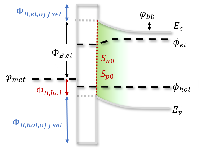
For the MS case, the current transport of electrons and holes over the boundary is governed by thermionic emission (TE): \[ J_{TE,el/hol}=A_0T^2 \exp\left(-\frac{\Phi_{B,el/hol}+\Delta\phi_I}{V_t}\right) \left(\exp\left(\frac{\varphi_{met}-\phi_{el/hol}}{V_t}\right)-1\right) \] where \(\Phi_{B,el}+\Phi_{B,hol}=E_g\) are the Schottky barriers for electrons and holes, which sum equals the band-gap. By using the Schottky-Mott rule, the Schottky barrier can be calculated from the difference of the metal workfunction and the absorber’s electron affinity, however note that in reality the actual Schottky barrier is always substantially lower due to various barrier-lowering effects (see(Tung T. Raymond 2014)). The potential drop over the insulator \(\phi_I\) is zero for the MS case.
The current boundary condition is achieved by adding surface recombination: \[ J_{MS,el/hol}=J_{TE,el/hol}\pm J_{rec} \] The boundary condition for the electrostatic potential is given by defining the conduction band edge: \[ E_c=\varphi_{met}+\phi_{B,el} \] Note that Quokka3’s independent treatment of current transport over the boundary and surface SRH is different to other simulation tools, e.g., Sentaurus Device. There no surface SRH is allowed for an MS contact, and the \(S_{n0}\) and \(S_{p0}\) inputs are the “thermionic emission velocities.” The TE current when using an unscaled Richardson constant implies very high (∼\(10^7\) cm/s) thermionic emission velocities, which effectively results in high surface recombination, meaning that surface SRH should not additionally be applied. However, Quokka3 allows to disable the thermionic emission current for the minority carriers, rendering the effective recombination caused by thermionic emission to zero, which makes it then sensible to define surface recombination. While this is a less physical MS model, it is well suited to effectively describe a passivating contact by already resolving the interplay of band bending and surface recombination. A similar approach may fail when “misusing” the thermionic emission velocities for the same purpose, as those are not SRH input parameters. Consider the extreme example: setting \(S_{n0}\) and \(S_{p0}\) to very low values results in a highly non-ohmic thermionic emission contact resistivity for majority carriers, and consequently, S-shaped J–V curves, but may be an excellent contact in Quokka3 when disabling minority thermionic emission.
The implementation of the MS boundary condition in Quokka3 further allows to consider the influence of a semiconductor buffer layer in a very simplistic way. Assuming that the buffer layer does not cause any transport limitations, the thermionic emission barriers are increased by the respective band offsets, \(\phi_{B,el,offset}\) and \(\phi_{B,hol,offset}\), to account for the shift of the TE barrier interface; see Fig. 2. Those offsets are added to the respective thermionic emission barrier, but not to the electrostatic potential boundary, meaning that the band bending in the absorber is unaffected.
MIS case (direct tunneling contact)
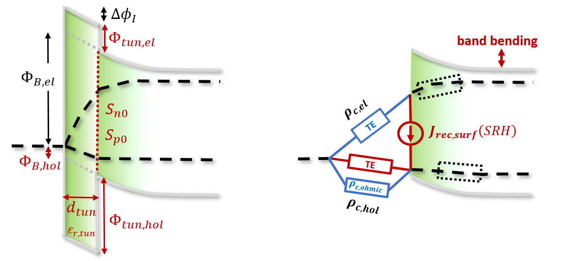
Additional to the MS case, the MIS case considers a thin insulator layer between the metal and the absorber via a simple direct tunneling model. A rectangular tunneling barrier is assumed characterized by the barrier thickness \(d_{tun}\) and barrier height \(\Phi_{tun}\). The resulting tunneling probability \(P_{tun}\) scales the TE current: \[ J_{MIS,el/hol}=P_{tun,el/hol}J_{TE,el/hol}\pm J_{rec}\left(+J_{ohmic}\right) \]
\[ P_{tun,el/hol}=\exp\left(-\frac{2d_{tun}\sqrt{2\,q\,m_{tun,el/hol}^*\left(\Phi_{tun,el/hol}-\Delta\phi_I/2\right)}}{\hbar}\right) \] Compared to the MS case, the band bending in the absorber is reduced by the potential drop over the insulator layer \(\Delta\phi_I\) , expressed via the electric field at the absorber surface \(E_{MIS}\) being a function of the permittivity ratio: \[ \vec{E}_{MIS}=\frac{\Delta\phi_I}{d_{tun}}=\frac{\varepsilon_{r,tun}}{\varepsilon_{r,skin}}\times\frac{\varphi_{met}+\Phi_{B,el}-E_{c}}{d_{tun}} \]
The insulator potential drop \(\Delta\phi_I\) also impacts the thermionic emission current by increasing the thermionic emission barrier.
Furthermore, one can define an ohmic contact resistivity \(\rho_{c,ohmic}\) in parallel to the majority carrier thermionic emission / tunneling current path, adding \(J_{ohmic} = \frac{\varphi_{met}-\phi_{el/hol}}{\rho_{c,ohmic}}\) to the majority carrier transport boundary condition. It can account for lateral inhomogeneities and / or pinholes resulting in an ohmic contact fraction. Note that this is not (yet) sufficient to properly model arbitrarily mixed tunneling–pinhole contacts as the influence of the ohmic contact fraction on the recombination is not considered.
MIS_simple (for lumped skins only)
Lastly, Quokka3 offers a further simplified MIS model available for lumped skins, either for their vertical resistance, i.e. between the bulk and the skin, or for the contact resistance to the metal. It is thus NOT a boundary condition available for the 1D detailed solver.
The MIS_simple case simplifies the full MIS case by assuming the the insulator potential drop to be zero, and always disables minority carrier transport. This makes the majority thermionic emission current solely a function of the quasi-Fermi levels, and not the electrostatic potential anymore, and is this suitable as a boundary condition for the quasi-neutral solver. The band-bending is then NOT resolved. The MIS_simple model solely accounts for a non-ohmic resistance effect, while recombination is still defined via lumped properties.
This might be a useful approach for passivating contacts for the typical case that the non-ohmic resistance effect should be accounted for, however the detailed interface properties are not known precisely and thus modeling recombination by a lumped approach is preferable. Finally, the MIS_simple model is also compatible with the ohmic mode, enabling to simulate resistance structures with MIS-type contacts.
Quasi-neutral boundary condition
The quasi-neutral boundary condition is applied on the (quasi-neutral) bulk-side of a skin when using the skin solver to solve a detailed skin only. A given Fermi-level split and the electrical potential calculated numerically by assuming quasi-neutrality is applied: \[ \phi_{el}-\phi_{hol}=\phi_{split} \]
\[ \varphi_{e,b}=\varphi_{e,qn}(\phi_{split}) \]
Parameterizing detailed skins: skin solver
The skin solver is the 1D detailed solver applied to a detailed skin only, using a quasi-neutral boundary condition on the bulk-side. The main purpose is to determine the lumped parameters representing the detailed skin, e.g. determine the \(J_{0,skin}=J_{0e}\) and \(R_{sheet}\) of a phosphorus emitter diffusion.
To solve a skin domain, an operating point needs be defined by the bulk-side Fermi-level split and the net current density through the skin. From the solution, the lumped parameters of the general parameterization which exactly represent the skin’s operating point, are extracted as follows:
- \(1/R_{sheet}\) is calculated for each carrier type by integrating the conductivity. The lower \(R_{sheet}\) determines the majority carrier type, i.e. whether the skin is ‘n-type’ or ‘p-type’. Quokka3 issues a warning if both types have low \(R_{sheet}\), which may lead to inaccuracies within multiscale modeling and should not happen in typical silicon solar cell skins.
- \(J_{G,skin}\) is found by integrating the generation rate (if the skin is illuminated)
- The skin potential \(\varphi_{skin}\) is assigned the majority potential of the mesh element with the highest majority carrier conductivity (usually the mesh element next to the surface).
- The vertical resistance \(\rho_{skin}\) is calculated by the difference of the skin potential and the bulk-side majority carrier quasi-Fermi potential over the net current density.
- The total recombination current density \(J_{rec,light}\) is determined by integrating volume recombination and adding interface recombination.
- If the skin is illuminated a second simulation in the dark simulation is performed.
- The total recombination current density \(J_{rec,dark}\) is determined by integrating volume recombination and adding interface recombination (which (only) in the dark equals the minority carrier current density through the bulk-side boundary).
- Any additional recombination in the illuminated case compared to the dark case is attributed to carriers generated within the skin, so that the collection efficiency is defined as: \[ \eta_c=1-\frac{J_{rec,light}-J_{rec,dark} }{J_{G,skin}} \]
- Consistent with above, \(J_{0,skin}\) for both the illuminated and dark case is defined as: \[ J_{0,skin}= \frac{J_{rec,dark}}{\exp\left(\phi_{split}⁄V_t\right)-1} \] Note that different to some other available software tools providing a similar functionality, Quokka3 does not assume quasi-neutrality within the skin, and thus also includes the space-charge-region (SCR) if present. While this might not make much difference for e.g. typical highly doped near-surfaces like emitter diffusions, the results are more accurate in general.
Multiscale solver
The multiscale solver couples the “small scales” of the skins using the skin solver with the qn-bulk solver solving the “large scale” 3D geometry. It used whenever a skin is defined via its detailed instead of its lumped properties. Then the skin solver is used to parameterize the respective skin and use the lumped parameters as boundary conditions for the qn-bulk solver subsequently simulating the 3D geometry.
Coupling degree
Quokka3 supports 3 different degrees of coupling a detailed skin to the qn-bulk which enables the user to balance speed vs. accuracy:
- single point: simulates and parameterizes the skin once at a single operating point, and assumes the parameters to be constant. This is fastest and most robust, and is well valid e.g. for highly doped near-surfaces like e.g. diffused emitters or Al-BSF, which usually have a constant \(J_{0,skin}\) and a negligible vertical resistivity.
- injection dependent recombination: simulates and parameterizes the skin for the required range of bulk-side Fermi-level splits and a at constant (and low) net current density. This is useful e.g. for lowly-doped surfaces passivated by a layer with moderate charge, which can show significant injection dependence of the recombination, but where vertical resistance is not relevant. This option should also be considered for typical doped near-surfaces, like e.g. light emitters, to increase accuracy.
- full coupling: simulates and parameterizes the skin for all relevant operating points. This is the generally valid and thus the most accurate option, but at the expense of simulation time. The general coupling is required e.g. to correctly account for resistive losses in the space-charge-region (SCR).
Texture multiplier
In Quokka3 the surfaces of the model domain are always strictly planar, a simplification used also for the vast majority of silicon solar cell device simulations with other tools. A complication arises when the actual surface is textured. This generally increases the effective recombination of such a textured skin due to the surface area enlargement. When assuming perfectly conformal skin properties along the textured surface (which is not necessarily a good assumption, but not to be discussed here), one could expect the recombination to scale with the geometric surface area enlargement (e.g. ~1.7 for random pyramid texture). However, due to current transport limitations within the pyramidal volume, a lower increase of e.g. \(J_{0,skin}\) is typically measured, see e.g. (Baker-Finch et al. 2012).
For lumped skin modeling this states no problem, as the required lumped properties can be measured on textured surfaces. For detailed skin modeling (and subsequent multiscale modeling) using a planar surface however, the recombination needs to be increased to represent the textured case. This is usually done by scaling surface recombination (and sometimes Auger) by such a factor, that the experimentally measured increase of \(J_{0,skin}\) (textured vs. planar) is replicated. While this is suitable to result in the correct effective recombination (i.e. matching \(V_{oc}\)), it leads to an unphysical distribution of the recombination. This is in particular noticeable in the skin’s collection efficiency (i.e. the IQE): due to the conformal assumption the a correct modelling of collection efficiency must use the actual surface recombination, and increasing it leads to an unphysical decrease of skin’s collection efficiency. Therefore a single fully detailed cell simulation can not simultaneously predict \(J_{0,skin}\) (\(V_{oc}\)) and collection efficiency (\(J_{sc}\)).
The multiscale model of Quokka3 however can resolve this problem: as both \(J_{0,skin}\) and collection efficiency are available as separate intermediate results, the texture multiplier is applied to \(J_{0,skin}\) skin only. Note this definition of the texture multiplier is different to the common definition (which increases physical recombination parameters). Next to the advantage described above, Quokka3’s definition can be considered the practically more meaningful one, as it is the directly measurable increase of effective surface recombination, i.e. \(\frac{J_{0,skin,textured}}{J_{0,skin,planar}}\).
Material properties
List of symbols
Note that the units are chosen to be consistent, but are not necessarily equal to the units of the corresponding input parameters of the settingsfile.
| symbol | unit | description |
|---|---|---|
| \(A_0\) | \(Acm^{-2}K^{-2}\) | Richardson constant |
| \(A_G\) | absorbed fraction of photons being transmitted through the illuminated surface | |
| \(c_{an}\), \(c_{cat}\) | \(cm^{-3}\) | anion, cation density |
| \(\vec{E}\) | \(V/cm\) | electric field |
| \(E_b\) | \(V/cm\) | electric field at boundary |
| \(E_g\) | \(eV\) | band gap |
| \(E_c\), \(E_v\) | \(eV\) | conduction band edge and valence band edge |
| \(f_t\) | occupied trap density fraction | |
| \(G\) | \(cm^{-3}s^{-1}\) | generation rate of electron-hole pairs |
| \(\vec{J}_{el}\), \(\vec{J}_{hol}\), \(\vec{J}_{an}\), \(\vec{J}_{cat}\) | \(A/cm^2\) | charge carrier current density |
| \(J_{cont}\), \(J_{pad}\) | \(A/cm^2\) | current density through contact and between metal and pad layer |
| \(k_B\) | \(VAs/K\) | Boltzmann constant |
| \(l_1\) | \(cm\) | optical pathlength of first path through the device |
| \(m_{tun}^*\) | \(kg\) | electron or hole tunneling mass |
| \(N_{0,an}\), \(N_{0,cat}\) | \(cm^{-3}\) | average / initial homogenous anion and cation concentration |
| \(N_A\), \(N_D\) | \(cm^{-3}\) | acceptor and donor density |
| \(N_c\), \(N_v\) | \(cm^{-3}\) | density of states in conduction band, valence band |
| \(N_t\) | \(cm^{-3}\) | total trap or defect density |
| \(n\) | \(cm^{-3}\) | electron density |
| \(\vec{n}\) | normal vector on boundary | |
| \(n_i\) | \(cm^{-3}\) | intrinsic carrier density |
| \(n_t\) | \(cm^{-3}\) | occupied trap density |
| \(p\) | \(cm^{-3}\) | hole density |
| \(Q_s\) | \(cm^{-2}\) | surface charge |
| \(q\) | \(As\) | elementary charge |
| \(R\) | \(cm^{-3}s^{-1}\) | recombination rate of electron-hole pairs |
| \(R_{front,avg}\), \(R_{rear,avg}\) | average (meaning n-th pass) internal reflectance | |
| \(R_{front,spec}\) | specular internal reflectance at front side | |
| \(R_{front,1}\) | first pass internal reflectance at front side | |
| \(R_{sheet}\) | \(\Omega\) | sheet resistance |
| \(S_{n0}\), \(S_{p0}\) | \(cm/s\) | fundamental electron and hole surface recombination velocity |
| \(T\) | \(K\) | temperature |
| \(T_1\), \(T_2\), \(T_n\) | (effective) transmission of first, second and n-th pass (internal optics) | |
| \(T_{ext}\) | transmitted fraction of external light through the surface | |
| \(V_{int}\) | \(V\) | internal voltage = ‘n-type’ polarity applied voltage |
| \(V_t\) | \(V\) | thermal voltage, equals \(k_BT/q\) |
| \(W\) | \(cm\) | device thickness |
| \(Z\) | (spectrally dependent) pathlength enhancement factor | |
| \(Z_0\), \(Z_\infty\), \(Z_p\) | \(Z\) parameters | |
| \(\alpha\) | \(cm^{-1}\) | absorption coefficient |
| \(v_{th}\) | \(cm/s\) | thermal velocity |
| \(\delta E_{BGN,c}\), \(\delta E_{BGN,v}\) | eV | band gap narrowing of conduction band and valence band |
| \(\varepsilon_0\) | \(AsV^{-1}cm^{-1}\) | vacuum permittivity |
| \(\varepsilon_r\) | relative permittivity | |
| \(\zeta\) | \(cm\) | closest distance to surface coordinate |
| \(\eta_c\) | collection efficiency | |
| \(\Theta_{surf}\), \(\Theta_{bulk}\) | angle of optical path relative to (textured) surface, and (planar) bulk, respectively | |
| \(\Theta_1\) (\(=\Theta_{bulk}\)), \(\Theta_2\), \(\Theta_n\) | first, second and n-th pass path-angle (internal optics) | |
| \(\kappa_{el}\), \(\kappa_{hol}\), \(\kappa_{an}\), \(\kappa_{cat}\) | \(AV^{-1}cm^{-1}\) | charge carrier conductivity |
| \(\Lambda_{rear}\) | Lambertian fraction of rear side (internal optics) | |
| \(\lambda\) | \(nm\) | wavelength |
| \(\mu_{el}\), \(\mu_{hol}\), \(\mu_{an}\), \(\mu_{cat}\) | \(cm^2V^{-1}s^{-1}\) | charge carrier mobility |
| \(\rho_{cont}\), \(\rho_{pad}\) | \(\Omega cm^2\) | skin - metal and metal - pad contact resistivity |
| \(\sigma_n\), \(\sigma_p\) | \(cm^{-2}\) | electron and hole capture cross section |
| \(\tau_{n0}\), \(\tau_{p0}\) | s | fundamental SRH electron and hole lifetime |
| \(\Phi_B\) | \(eV\) | Schottky barrier height |
| \(\phi_{el}\), \(\phi_{hol}\), \(\phi_{an}\), \(\phi_{cat}\) | \(V\) | charge carrier electrochemical potential (=quasi-Fermi potential) |
| \(\phi_{maj}\) | \(V\) | quasi-Fermi potential of majority carriers |
| \(\phi_{split}\) | \(V\) | quasi-Fermi potential split |
| \(\varphi_e\), \(\varphi_{skin}\), \(\varphi_{met}\), \(\varphi_{pad}\) | \(V\) | electrostatic, skin, metal and pad potential |
| \(\Delta\varphi_{maj}\) | \(V\) | difference between skin potential and bulk-side majority quasi-Fermi potential |
References
Altermatt, Pietro P. 2011. “Models for Numerical Device Simulations of Crystalline Silicon Solar Cells—a Review.” Journal of Computational Electronics 10 (3): 314–30. https://doi.org/10.1007/s10825-011-0367-6.
Baker-Finch, Simeon C., Keith R. McIntosh, Mason L. Terry, and Yimao Wan. 2012. “Isotextured Silicon Solar Cell Analysis and Modeling 2: Recombination and Device Modeling.” IEEE Journal of Photovoltaics 2 (4): 465–72.
Basore, Paul A. 1993. “Extended Spectral Analysis of Internal Quantum Efficiency.” In 23rd Photovoltaic Specialists Conference, 147–52. IEEE; IEEE.
Brendel, R., M. Hirsch, R. Plieninger, and J. J. H. Werner. 1996. “Quantum Efficiency Analysis of Thin-Layer Silicon Solar Cells with Back Surface Fields and Optical Confinement.” IEEE Transactions on Electron Devices 43 (7): 1104–13.
Brendel, Rolf. 2012. “Modeling Solar Cells with the Dopant-Diffused Layers Treated as Conductive Boundaries.” Progress in Photovoltaics: Research and Applications 20 (1): 31–43. https://doi.org/10.1002/pip.954.
Clugston, D. A., and P. A. Basore. 2010. “PC1D Version 5: 32-Bit Solar Cell Modeling on Personal Computers.” In 35th Photovoltaic Specialists Conference, 207–10. IEEE. https://doi.org/10.1109/pvsc.1997.654065.
Fell, A. 2013. “A Free and Fast Three-Dimensional/Two-Dimensional Solar Cell Simulator Featuring Conductive Boundary and Quasi-Neutrality Approximations.” IEEE Transactions on Electron Devices 60 (2): 733–38. https://doi.org/10.1109/ted.2012.2231415.
Fell, A., F. Feldmann, C. Messmer, M. Bivour, M. C. Schubert, and S. W. Glunz. 2018. “Adaption of Basic Metal–Insulator–Semiconductor (Mis) Theory for Passivating Contacts Within Numerical Solar Cell Modeling.” IEEE Journal of Photovoltaics. https://doi.org/10.1109/JPHOTOV.2018.2871953.
Fell, Andreas, Keith R. McIntosh, and Kean C. Fong. 2016. “Simplified Device Simulation of Silicon Solar Cells Using a Lumped Parameter Optical Model.” IEEE Journal of Photovoltaics, 1–6. https://doi.org/10.1109/JPHOTOV.2016.2528407.
Fell, Andreas, Jonas Schoen, Martin C. Schubert, and Stefan W. Glunz. 2017. “The Concept of Skins for Silicon Solar Cell Modeling.” Solar Energy Materials and Solar Cells, 173 (Supplement C): 128–33. https://doi.org/10.1016/j.solmat.2017.05.012.
Green, Martin A. 2002. “Lambertian Light Trapping in Textured Solar Cells and Light–Emitting Diodes: Analytical Solutions.” Progress in Photovoltaics: Research and Applications 10 (4): 235–41.
Macdonald, Daniel, and Andrés Cuevas. 2003. “Validity of Simplified Shockley-Read-Hall Statistics for Modeling Carrier Lifetimes in Crystalline Silicon.” Physical Review B 67 (7): 075203.
McIntosh, K. R., and S. C. Baker-Finch. 2015. “A Parameterization of Light Trapping in Wafer-Based Solar Cells.” IEEE Journal of Photovoltaics PP (99): 1–8. https://doi.org/10.1109/JPHOTOV.2015.2465175.
Rand, James A., and Paul A. Basore. 1991. “Light-Trapping Silicon Solar Cells-Experimental Results and Analysis.” In 22nd Photovoltaic Specialists Conference, 192–97. IEEE; IEEE.
Shockley, We, and W. T. Read Jr. 1952. “Statistics of the Recombinations of Holes and Electrons.” Physical Review 87 (5): 835.
Tung T. Raymond. 2014. “The Physics and Chemistry of the Schottky Barrier Height.” Applied Physics Reviews 1 (1): 011304. https://doi.org/10.1063/1.4858400.