Highlights
- Specifically developed for silicon solar cells, therefore easy-to-understand settings and output for researchers and engineers in this field
- By far fastest tool for simulating 2D / 3D carrier transport in silicon solar cell devices, enabled by the skin concept and optimized C++ code
- Intrinsically accounts for large-area effects like e.g. distributed metal resistance, edge recombination or process inhomogoneities, without the need for complicated approaches like e.g. coupling with SPICE simulations
- First-principles luminescence modelling from 3D electrical solution gives PL, EL and hyperspectral images with unmatched accuracy
- Includes 1D detailed solver for semiconductor carrier transport NOT employing quasi-neutrality (PC1D-equivalent), featuring ion transport for perovskite cells and a transient solver
- Skin solver to solve a non-neutral skin domain in 1D and parameterize the results into lumped properties (e.g. diffused emitter into \(J_{0,skin}\))
- Multiscale solver: generic and fully automated coupling of the 1D skin solver and the 3D qn-bulk solver, enabling fast 3D cell simulations including the details of the skins
- Cloud computing: very high simulation speed on any computer, no dedicated high performance hardware required, conveniently run large simulations while your computer is shutdown
- Support by the software developer and leading solar cell modelling expert
Feature description
This section provides a brief description of the main features of Quokka3. See the User Guide and Modelling Guide for an in-depth description.
Modelling concept
In Quokka3 a solar cell is conceptualized into separate regions:
The bulk: it is the main absorber, and (for Si solar cells) can well be assumed to be everywhere quasi-neutral if defined to exclude the near-surface regions. Only the bulk is discretized in the depth coordinate.
The skin layer: skins are region-wise homogenous areas which cover everything between the quasi-neutral bulk and either the actual surface or the contact to the metal. Typical skins are contacted or non-contacted diffused surfaces, or passivated surfaces (including the inversion or accumulation layer). In Quokka3, skins can be defined via their lumped or detailed input parameters
The contact layer: contacts in Quokka3 define the interface where current can flow between the skin and the metal. Where no contact is defined between the skin and the metal layer, they are assumed to be perfectly isolated.
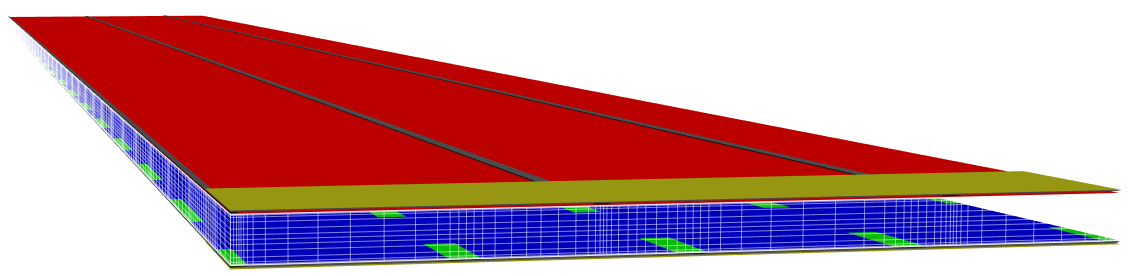
The metal layer: represents finger and busbar geometry and accounts for lateral current flow within them
The pad layer: pads represent the probes or solder pads to which the plus and minus pole is applied, and through which the current is extracted. They are important only when solving current transport in the metal layer, because otherwise the entire metal geometry effectively represents a probe applying a constant potential.
The key of Quokka3 to make it numerically efficient and specifically useful for wafer-based silicon solar cells, is to numerically treat the skins always as a parameterized boundary condition when solving carrier transport in the bulk. The main lumped parameters to describe a skin as a boundary condition are its recombination property \(J_{0,skin}\), and its sheet resistance \(R_{sheet}\), which are well-established to sufficiently describe a Si solar cell in many cases. Quokka3 notably can also model skins in detail and then use a more general parameterization, which is applied in the multiscale approach ensuring high accuracy also for arbitrary skin properties.
Quokka3 uses a structured, orthogonal and non-equidistant mesh to discretize the solution domain and build the finite differences expressions. This means that the solution domain is always strictly cuboidal, and that the geometry definition of the device needs to consists of primitive rectangular geometric features aligned to the coordinate axis. The geometric features are arbitrary in number, position and size, resulting in a generic geometry definition within this rectangular restriction. As an exemption from this a circle as a primitive shape is also supported. It is however recommended in most cases to instead use a square shape with equal area, which requires a much smaller mesh for accurate discretization. The orthogonal mesh is well suited for silicon solar cells, as most cases of interest can be approximated by rectangular device geometries. It comes with the benefits of a rapid and fully automated meshing algorithm (seconds for millions of elements) requiring no attention from the user, and fast and robust electrical solver numerics based on finite differences.
Qn-bulk solver
Simplified semiconductor transport model
The separate treatment of the skins comes with two decisive benefits opposed to the generic approach of fully solving the semiconductor equations in the entire device:
The volume of the skin is not discretized, resulting in a much smaller mesh for a given geometry
The remaining bulk to be solved inhibits a lower complexity of physics to be solved. In particular being able to employ the quasi-neutrality approximation omits the need to solve the Poisson equation (which is not to be mistaken with the low-injection approximation: the qn-bulk solver correctly models any injection level and does result in a correct non-zero electric field in the bulk).
As a result from the above, the numerical problem is orders of magnitude easier to solve compared to full discretization including the details of the skin. By employing specifically developed C++ code for the finite-differences method and PETSC [ref] for the low-level number crunching, the qn-bulk solver handles several millions of elements on standard computer hardware in manageable times (hours). This performance (memory usage and simulation time for a given mesh size) is comparable to other state-of-the-art commercial numerical simulation software, and outperforms Quokka2 by up to 2 orders of magnitude. Combined with the skin concept, Quokka3 is the only tool on the market practically capable to solve large solar cell geometries up to full-area solar cells in 3D.
Being sensible for such large geometries opposed to the common unit-cell simulations, the qn-bulk solver can include an additional conductive layer on top of the skin layer to represent current transport in the metal. This way, the generally distributed resistive effects of the metallization are fully accounted for in the single 3D solution domain, omitting the need to separately determine a less accurate lumped \(R_{series}\), or the high effort of coupling with subsequent SPICE simulations.
Currently, the qn-bulk solver only supports steady-state simulations.
Ohmic mode
As a further simplified subset of the qn-bulk solver, Quokka3 supports solving a single current transport equation for a single potential, assuming constant values and equal polarities for volume resistivities, sheet resistances and contact resistivities. That means the device is considered purely ohmic, i.e. ignores any doping types (n-type or p-type), and consequently does not account for diode-behaviour, carrier densities, generation and recombination.
The ohmic mode is able to simulate resistance test structures like e.g. the transfer-length-method (TLM). It is particular useful if the test-structure geometry can not be accurately described by analytical formulas, or if the influence of artefacts like e.g. perimeter regions should be included.
1D detailed solver
Complementary to the qn-bulk solver, in Quokka3 a 1D electrical solver for the full semiconductor equations not employing quasi-neutrality is implemented. The 1D detailed solver features state-of-the-art models for solving general semiconductor physics in silicon.
Next to silicon, a second area of focus for Quokka3 is modelling perovskite cells, which require some additional physics to be accounted for, in particular ion transport.
Currently, the 1D detailed solver features the following:
- Fully coupled solution of semiconductor equations in 1D in a single material (no interfaces)
- Ideal, Metal-Semiconductor (MS / Schottky) and Metal-Insulator-Semiconductor (MIS) contact physics
- Surface charge
- Surface SRH
- Fermi-Dirac statistics, injection-dependent band-gap-narrowing, incomplete ionization
- Both steady-state and transient (beta) mode
- Custom material properties
- Steady-state and transient ion transport (for perovskite cells) (beta)
- Transient, i.e. general SRH model (trapping) (beta)
In development and planned to be released until 2019 are the following
- multiple layers of different custom semiconductor materials, including multijunction layers
- interface physics: bifacial SRH, simple tunneling models (ideal, lumped resistance or via recombination)
Detailed cell
The 1D detailed solver can be used to solve a semiconductor device (i.e. a solar cell) in 1D. This closely resembles the functionality of the well-known PC1D software.
Skin solver
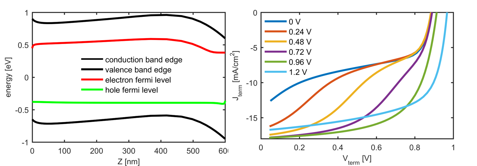
The 1D detailed solver can also be used to solve a skin domain in 1D and parameterize the results into lumped skin properties. Here, to the bottom of the domain a quasi-neutral boundary condition is applied. A steady-state operating point of the skin is then defined by the Fermi level split at the quasi-neutral boundary, and the net current through the skin. The skin solver can then generally parameterize the results of the detailed simulation into the lumped properties exactly describing this operating point of the skin. These lumped parameters are suitable for the qn-bulk solver as a boundary condition.
The most prominent usage scenario for the skin solver is to simulate a near-surface region of a silicon cell, e.g. a diffused emitter, and simulate the \(J_{0,skin}=J_{0e}\) for a user-defined profile and surface recombination. It can also be used to simulate the effective contact resistance and injection dependent recombination of a Schottky-type contact.
By varying both the Fermi level split and the net current in the relevant range, any skin can be accurately described for any operating point of the solar cell it is implemented in using the general parameterization. This works as long is it is valid to describe a skin in quasi-1D, and is naturally subject to successful convergence.
Optical solver
Illumination
Quokka3 does not (yet) support detailed optical modeling of a solar cell device based on surface morphology and thin film properties.
It supports importing generation profiles defined by the user, and also a simple and rapid spectrally resolved optical model based on the lumped optical input parameters front surface transmission \(T_{ext}\) and the pathlength enhancement \(Z\), the latter quantifying the device’s light trapping capability. This so called TextZ model was shown to be accurate for wafer-based silicon solar cells and has the following benefits:
It is a good way to import results from other optical modeling tools, as the required inputs can be easily extracted from most common ray tracers
The input parameters are, to good approximation, independent of:
- the incident spectrum, enabling accurate quantum efficiency simulations (opposed to when importing a generation profile),
- the device thickness, allowing variation of the same without having to redo detailed optical simulations,
- the device temperature, again allowing variation of the same without having to redo detailed optical simulations.
For 2D and 3D simulations, shading of the metal geometry is considered. Here the user can define a “shading fraction” to account for <100% shading due to the fact that light hitting metal can still find its way into the cell via reflections and scattering.
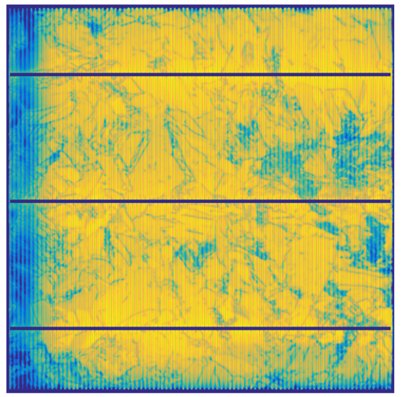
Luminescence
Having the full 1D-3D distribution of Fermi level splits handy as a result from the electrical solver, it is straightforward to calculate spontaneous emission at every point using Planck’s law. Reabsorption and internal reflections are handled by a statistical emission function, resulting in a luminescence spectrum at every point of the surface. With a known spectral sensitivity of the optical system and detector, this hyperspectral map is then converted into a luminescence intensity map.
As non-uniform carrier densities, both laterally and depth-wise, and re-absorption are fully accounted for, the resulting EL / PL images are valid for any operating point of the cell imposing minimal simplifications. For example, the relatively high signal for \(J_{sc}\) luminescence images caused by the built-in potential are correctly simulated.
By iteratively coupling the electrical solver with the luminescence solver photon recycling can be addressed. In each step the reabsorbed photons from the luminescence solver are added to the generation rate. This feature is planned to be released late 2018.
Multiscale solver
In Quokka3 multiscale modeling means that one or more skins are defined by detailed (not lumped) inputs, solved in 1D by the skin solver, parameterized, and coupled to the qn-bulk solver as boundary conditions. The main advantage is a substantially improved computational speed compared to a full detailed 3D simulation of the entire domain, while not compromising accuracy when using the general skin parameterization for typical silicon solar cell skins. For medium to large mesh sizes of the qn-bulk solver, the skin-solver does not add significantly to the overall speed, meaning that the capability to solve large geometries can fully be used within the mutliscale modeling.
Notable there are three different degrees of complexity to couple a skin-solver to the qn-bulk solver:
single-point coupling: the skin is solved once only for a representative operating point to derive constant values for the skin parameters. This requires the least computational effort, is most robust, and is valid for typical skins including high doping or high charge. This essentially means deriving single values for \(J_{0,skin}\) and \(R_{sheet}\), i.e. using the standard conductive boundary model.
injection dependent coupling (beta): the skin is solved for the relevant range of quasi-Fermi level splits, but at a constant net current density. This is best for skins which do show significant injection-dependent recombination but low (or constant) vertical resistance (e.g. passivation with moderate charge)
full coupling (beta): the skin is solved for the full relevant range of the quasi-Fermi level split and the net current density. It is costlier in terms of computational demand and more susceptible to convergence problems, but is the generally valid approach for any skin properties. Improved robustness of this coupling mode is currently ongoing towards making it the robust default choice.
In summary, the multiscale solver has the following benefits:
It’s fully automated, meaning the user defines his domain including the details of the skin equivalent to a full detailed simulation, but benefits from the vastly improved speed.
The automated coupling within a single tool ensures consistent optical modeling and consideration of imperfect skin collection efficiency, which is difficult to ensure when coupling manually using different tools.
Within a single simulation, different skins can individually be described by lumped inputs or detailed inputs. E.g. one can vary the doping profile of the non-contacted front emitter while assuming a lumped \(J_{0,skin}\) for the contacted emitter regions and the rear contacts.
When approximating a textured surface by a planar solution domain, a texture multiplier can be applied exclusively to bulk-side recombination without affecting the short-wavelength collection efficiency, which is an unavoidable inconsistency in full detailed simulations.